| 1)Connector: | Nickel plated 15 Pin male to male |
| 2)Cable: | made of 75ohms mini coax video wire, using individually shielded 28-gauge coaxial wire. 3+2/3+4/3+6/3+8/3+9 is all right. |
| 3)Length: | 3m |
| 4)Color: | Black/white |
| 5)Application: | This male VGA to male VGA cable is designed for connecting video card outputs to monitors directly. Most modern flat panel displays require this type of cable |
| 6)Packaging: | PE bag |
| 7)Support: | ODM/OEM service |
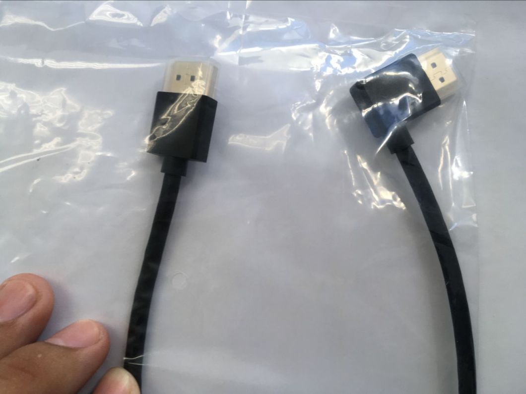
 Cheaper 3m black 15Pin VGA Male to Male Cable
| 1)Connector: | Nickel plated 15 Pin male to male |
| 2)Cable: | made of 75ohms mini coax video wire, using individually shielded 28-gauge coaxial wire. 3+2/3+4/3+6/3+8/3+9 is all right. |
| 3)Length: | 3m |
| 4)Color: | Black/white |
| 5)Application: | This male VGA to male VGA cable is designed for connecting video card outputs to monitors directly. Most modern flat panel displays require this type of cable |
| 6)Packaging: | PE bag |
| 7)Support: | ODM/OEM service |
Â
HDI PCB Specification
High density interconnect (HDI) PCBs represent one of the fastest-growing segments of the printed circuit board market. Because of its higher circuitry density, the HDI PCB design is able to incorporate finer lines and spaces, smaller vias and capture pads, and higher connection pad densities. A high density PCB features blind and buried vias and often contains microvias that are .006 in diameter or even less.
HDI PCBs are characterized by high-density attributes including laser microvias, fine lines and high performance thin materials. This increased density enables more functions per unit area. Higher technology HDI PCBs have multiple layers of copper filled stacked microvias (Advanced HDI PCBs) which creates a structure that enables even more complex interconnections. These very complex structures provide the necessary routing solutions for today's large pin-count chips utilized in mobile devices and other high technology products.
The HDI PCBs we offer include the following highly requested characteristics:
Blind and/or buried vias
Via-in-pad
Through vias from surface to surface
20 µm circuit geometries
30 µm dielectric layers
50 µm laser vias
125 µm bump pitch processing
Applications
HDI PCB is used to reduce size and weight, as well as to enhance electrical performance of the device. HDI PCB is the best alternative to high layer-count and expensive standard laminate or sequentially laminated boards. HDI incorporate blind and buried vias that help to save PCB real estate by allowing features and lines to be designed above or below them without making a connection. Many of today's fine pitch BGA and flip-chip component footprints do not allow for running traces between the BGA pads. Blind and buried vias will only connect layers requiring connections in that area.
HDI PCB
HDI PCB,Special HDI PCB,HDI Prototype PCB,HDI Board PCB
Storm Circuit Technology Ltd , http://www.stormpcb.com