The traditional coin-operated telephones use several pairs of infrared emission and receiving pairs as sensors to measure the diameter of the coins by the principle of coin shading. This method has low precision and is less able to identify counterfeit coins of the same diameter but different materials.
A new generation of coin-operated telephones, such as the British sapphire series, can accurately detect the material, thickness and diameter of coins, so the accuracy and reliability are greatly improved. In this type of new coin-operated telephone, a micro-power consumption, a wide operating voltage range, and a high-performance single-chip microcomputer capable of adapting to telephone line power are needed as the core of intelligent detection and control. The MICROChip PIC16C71 microcontroller from the United States can meet this requirement and is inexpensive.
Its core PIC16C71 is a low-cost, high-performance, high-performance microcontroller with full-on-chip on-chip RAM, 2 KB of on-chip ROM, and four 8-bit on-chip A/D converters. With a 20 MHz clock, each instruction cycle is only 0.2μS. The 14-bit reduced instruction set (RISC) has a total of 35 high-efficiency instructions, mostly single-cycle instructions, which are more than four times faster than typical microcontrollers. The wide operating voltage range of 3 to 6 V and the micropower design (operating current is only 15 μA at 3V and 32 kHz, and the sleep holding current is less than 1μA), making it especially suitable for working environments powered by telephone lines, without the need for another With power supply. In addition, the machine also has a program security bit to prevent illegal copying, a "watchdog" (WDT) that prevents the program from "derailing" after being disturbed, and an I/O interface with strong load capacity, which can directly drive 20-25. The mA load greatly simplifies the system structure and improves reliability.
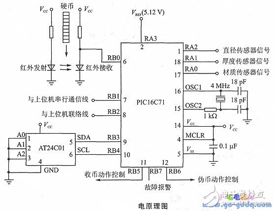
The AT24C01 is a new, high-performance serial rewritable read-only memory (E2 PROM) that is inexpensive. In this system, it is used to store the currency, currency value and corresponding material, thickness and diameter of the sensor signals. The information can be saved for 100 years after power failure, and the number of erasing can reach 100,000. The quiescent current is 30 μA, the capacity is 128 bytes, and the operating voltage is 2.6 to 6 V. Due to the serial operation mode, only two I/O lines are needed for data transfer, which is especially suitable for single-chip microcomputers with limited I/O line resources. Another advantage is that the currency, currency value and 3 sensor parameter values ​​can be modified "online". To adapt to different regions, countries and different coins. Although the PIC16C71 does not have an I2C BUS, it is easy to simulate the I/C BUS read/write timing with the software to complete the serial transfer of data.
Second, the power supply
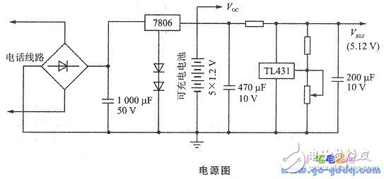
The power supply part of this system is shown in Figure 3-5. After the power from the telephone line is bridge rectified and filtered, it is regulated to 6.4 V by a three-terminal regulator, and five 5# rechargeable batteries (each 1.2 V) are floated and used as system power. . Normally, the system can be operated normally by the telephone line. When performing the action of collecting and rejecting counterfeit coins, the large current (about 15 mA) required for the high-sensitivity electromagnet is supplied by the rechargeable battery. In addition, the 6.4 V voltage is regulated to 5.12 V via a precision reference TL431, which is used as the parameter power supply vREF for A/D conversion. The RA port pin structure mode control bit of the PIC16C71 is set to PCFGl-0, PCFGO -1.
Take mode 01, at this time, the RAO, RA1, and RA2 pins are used as analog signal inputs, and RA3 is used as the input pin of the reference parameter voltage VREF.
Fourth, coin detection
For the detection of the thickness and diameter of the coin, a variety of existing sensors are available. The main points should be considered: small size, low price, and non-contact detection. We use a capacitor and eddy current sensor. The alloy content of the coin can be measured indirectly by detecting its specific gravity, resistivity, and permeability.
The signals from the above three sensors (material, thickness, diameter) are processed by amplification, phase discrimination, precision detection, filtering, temperature compensation, etc. to form a DC voltage signal of 0 to 5, 12 V, which is sent to the RAO of the PIC16C71 microcontroller. Three pins, RA1 and RA2, for fast A/D conversion.
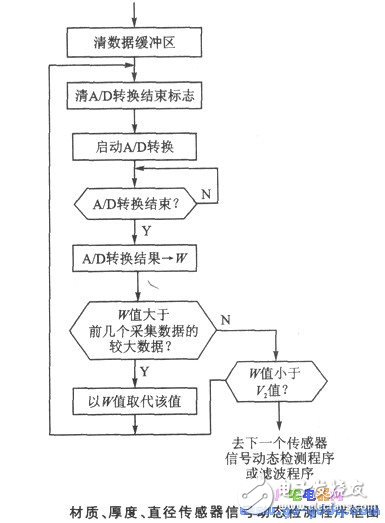
When power-on reset, the program starts from the OOOOH address, executes a jump instruction, and goes to the main program starting from O010H. Initialization is performed first, and then the SLEEP instruction enters the "sleep" micropower state to reduce power consumption. When the coin is put in from the coin-operated port, an interrupt request pulse signal is generated due to blocking the highly sensitive micro-infrared emission and receiving the optical path between the tubes. Its rising edge triggers the RBO (INT) terminal of the microcontroller, wakes up the microcontroller PIC16C71 from “sleep†and enters the interrupt service routine entry with address 0004H. Then, through a jump instruction at the place, it is transferred to a program module for detecting three sensor signals of material, thickness and diameter. The three sensors of material, thickness and diameter are arranged in a spaced order on the coin slide. In order to simplify the mechanical structure and increase the speed of detection, a method of dynamically detecting rolling coins can be employed. It has been experimentally determined that the signal voltages of the three sensors of material, thickness and diameter have a curved shape as shown in the following figure during the rolling process of the coin through the sensor.
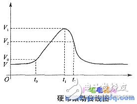
When the signal voltage rises to a certain threshold voltage Vo, it indicates that the coin has entered the sensor detection range. At this time, the data collected each time is compared with the previous one, and the larger one is stored in the on-chip RAM unit in order. When a signal is detected and the voltage drops to a certain threshold voltage V2, the coin has rolled away from the sensor. At this point the program moves to the detection of the next sensor signal. When all three sensor signals are detected, the program turns off the A/D and converts the digital filter to eliminate the influence of the interference glitch pulse, and obtains the maximum value Vl of the sensor signal. Then temperature compensation is performed, and the sensor no-load value V is subtracted from the V1 value to eliminate the temperature influence. After all three sensor signals have been processed, the program enters the identification module, and quickly scans various coin parameters (including material, thickness, and diameter) stored in the serial EPROM AT24C01. If the measured three parameters do not match the three parameters of the pre-stored various coins (beyond the upper and lower limits), it is considered to be a counterfeit coin. The RB6 pin of PIC16C71 outputs a signal to drive high-sensitivity, low-power fast electromagnetic. Iron action, push the counterfeit coins out of the raceway.
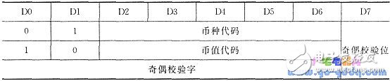
After identifying and confirming the coin, its currency and currency code are processed by parity, and then serially transmitted to the rate management host computer (such as 80C31, etc.) by the RB1 pin. The communication convention is asynchronous. The data structure is as follows. Shown. A set of data is sent for each coin, and each group consists of 3 data words. The format is shown in the table below.
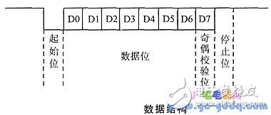
Currency currency code table
After each group of data is sent, the program converts RB1 from the output mode to the input mode, and queries the waiting rate to manage the response signal of the host computer. After receiving a set of data, the host computer will pull the data line low for the response signal within 1ms after the parity check is correct. After receiving the response signal, the PIC16C71 enters the SLEEP "sleep" state and waits for the next coin to wake up. If the host computer response signal is not received within 1ms, the PIC16C71 will repeat the data set. If no response signal is received after three consecutive transmissions, the program goes to the fault alarm.
When the coin is put into the specified value, the rate management host sends a signal via RB2 to wake up the PIC16C71 to perform the coin-receiving action, and then the PIC16C71 enters the "sleep" state.
According to the above principle. The following figure shows the main block diagram and the dynamic test block diagram. Due to space limitations, the program list is omitted.
The system makes full use of the high-performance instructions, fast AlD conversion, micro low power consumption, wide working voltage, strong load capacity, anti-interference watchdog performance and resources provided by the high-performance PIC16C71 microcontroller, which makes the system structure very simple. , high reliability, low cost, and satisfactory results in practical applications.

Kadena (KDA) is a hybrid blockchain network and smart contract platform that aims to unite public applications, private blockchains, and other interoperable chains in one place, driving traffic to the high-bandwidth computer at the heart of the Kadena public chain. Kadena`s mining algorithm is Blake2S, which supports ASIC mining.
Kadena is a blockchain network and smart contract token aiming to bring together both public applications and private blockchain.
The coin solves various problems that prevent blockchain adoption on a bigger scale. The protocol enables businesses and developers to make transactions and share information across many networks.
The Coin is actually on the grid to reduce users` experience in the network. Ethereum users experience a lot of network congestion which results in high gas fees.
A few changes have come into Kadena mining. A proof of work blockchain uses PACT to create smart contracts in the hidden gen. Therefore you need to know the following before mining Kadena. PACT is an intelligent contract language serving the needs of the blockchain community.
1.You Need an Excellent Mining Hardware
To mine efficiently, you will require suitable mining hardware. Kadena uses ASIC miners. But, unfortunately for Kadena miners, CPUs and GPUs are not usable. Furthermore, ASIC mining receives support from the Blake2S algorithm.
2.Make Sure You Have a Kadena Wallet Address
You will need a Kadena wallet address to receive and monitor your profit. F2pool also makes the distribution of the revenues to every user daily at 2KDA. The Kadena node wallet is a perfect wallet where you can receive your mined KDA. all you need to do is install it, click receive, and have a new wallet address.
You will need to configure your Asic Miner to a mining pool server for your hashrate and profit to be recorded and monitored.
3.Start Mining
After all the setting is done, your miner will be ready to work. Make sure you enter your wallet address and click on the go button to receive your revenue.
Kda Miner,Antminer Ka3 166Th,Bitmain Antminer Ka3 166Th,Antminer Bitmain Ka3
Shenzhen YLHM Technology Co., Ltd. , https://www.hkcryptominer.com