IGBT overview
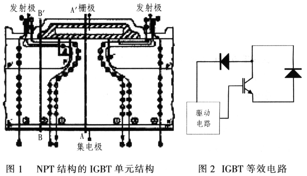
1.1 IGBT structure characteristics IGBT is a high-power, integrated "Insulated Gate Bipolar Transistor" (Insulated Gate Bipolar Transistor). It is a new type of composite electronic device developed in the early 1980s that combines the advantages of high-power bipolar transistors GTR and MOSFET FETs. It combines the high input impedance of MOSFETs with the low on-state voltage drop of GTR. Figure 1 shows the N-channel enhancement type vertical IGBT cell structure. The IGBT adopts a trench structure to reduce the on-state voltage drop and improve its frequency characteristics. And use NFT technology to achieve high power of IGBT. The IGBT uses a MOSFET as an input part, and its characteristics are N-channel enhancement type. The transfer characteristics of MOS devices are similar, forming a voltage-type drive mode, using GTR as an output component, and the on-voltage is reduced and the capacity is large. The difference is that the collector IC of the IGBT is controlled by the gate-emitter voltage UCE, and is turned on and off. The gate-to-shoot voltage UCE is determined.
At present, most of the inverters use IGBT and IPM as switching devices. The intelligent power module (IPM) consisting of the basic combination unit of IGBT and the driving, protection and alarm circuits has become the development direction of IGBT intelligentization. The protection circuit and some interface circuits and power circuits are integrated into one power device. The DC 600 V inverter of 35 kW class generally adopts 1 200 V/300 A module, IGBT and IPM are divided into single unit and double unit, and 3 double unit modules can form the main circuit of i phase inverter, as shown in Fig. 2. Show.
This article refers to the address: http://
1.2 Application of IGBT rail vehicles in power supply systems IGBT modules are widely used in rail vehicles to form traction constant current converters and constant voltage constant frequency (CVCF) inverters for auxiliary power systems. Foreign metro or light rail vehicle auxiliary systems use a variety of IGBT devices. For locomotive traction, Germany needs to develop a 1.7 kV IGBT for the 750 V grid and a 3.3 kV IGBT module for the 1 500 V grid, simplifying the structure of the traction inverter main circuit. Japan's 700 series electric vehicle set three-point main converter. With high-power flat-panel IGBTs (2 500 V/1 800 A), one IGBT component can be used for each leg of the rectifier and inverter, which makes the IGBT assembly simplified while the overall structure of the power unit is compact. .
In China's 200 km/h EMUs introduced by Alstom in France, the main converter switches use IGBT devices with a withstand voltage of up to 6 500 V/600 A, and the auxiliary converters use PWM technology with a switching frequency of 1 950 Hz. 3 sets of double IGBTs and related anti-parallel diodes, each of which forms one phase of three phases; Shanghai Rail Transit Line 3 vehicle is its auxiliary system consisting of IGBTs with voltage class of 330 V to form a 2-point inverter directly Inverter; the auxiliary system on the Guangzhou Metro Line 1 vehicle uses IGBT double direct-to-straight converter with high-frequency transformer to achieve electrical isolation; Shenzhen Metro Phase I uses 6 IGBT modules used as traction inverters and 2 for The IGBT module of the brake chopper completes the traction inverter function: the main circuit of Tianjin Binhai EMU adopts IGBT voltage type three-phase direct-inverting inverter, and the auxiliary power supply inverter adopts IGBT component inverter, and the switching capacity is 3 300 V/800 A.
2 IGBT application in DC 600 V
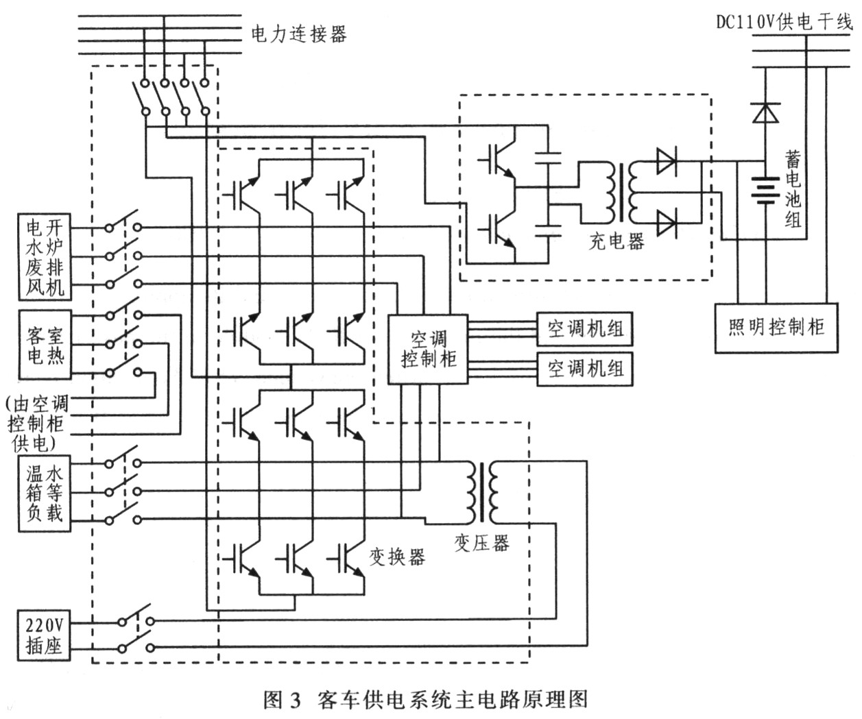
2.1 DC 600 V passenger car power supply system introduction DC 600 V air-conditioned passenger car power supply system uses locomotive centralized rectification, passenger car decentralized inverter mode, constitutes the entire train's AC and AC power supply system. The working process is as follows: the electric locomotive steps down, rectifies and filters the 25 kV grid single-phase AC power into DC 600 V to supply power to the passenger car. The bus converts the DC 600 V provided by the locomotive into single and three-phase AC according to the needs of the electric equipment. And DC 110 V. The system uses two independent power supplies. With a certain redundancy, the basic principle diagram of passenger car power supply is shown in Figure 3.
2.2 Application of IGBT in DC 600 V power supply system inverter The air conditioner bus uses two 35 kW inverters consisting of IGBT modules. The main circuit principle of the inverter is shown in Figure 4, mainly by the lower function module. constitute:
(1) Input and output isolation circuit composed of KMl and KM3 electromagnetic contactors. The main function is to isolate when the inverter, input circuit or output load fails, to prevent fault diffusion.
(2) The intermediate support circuit consisting of filter capacitors C1 and C2, the main function is to filter the voltage ripple of the input circuit, and make the DC voltage stable when the load changes. Since the power of the inverter is large, the capacity of the filter capacitor is large, and an electrolytic capacitor is generally used. Due to the dispersion of the parameters of the capacitor itself, the two capacitor voltages in series cannot be completely consistent. The method of using parallel voltage equalizing resistors at both ends of the capacitor, R1 and R2 in Fig. 4, the other function is to discharge the charge of the capacitor when the inverter stops operating.
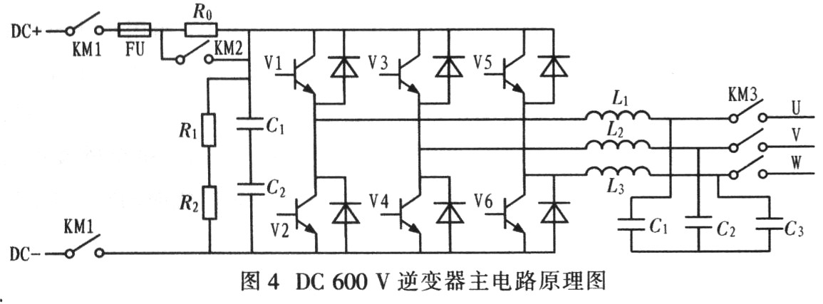
(3) A buffer circuit composed of R0 and KM2, the working principle is: when a voltage is applied to the input terminal, the capacitor is first charged through the buffer resistor R0. When the capacitor voltage is charged to a certain value (such as 540 V), KM2 pulls in and shorts R0. Only when the resistor R0 is short-circuited, the three-phase inverter circuit can start working.
(4) An AC filter circuit composed of L1 to L3 and C1 to C3 can convert the PWM wave output from the inverter into a quasi-sine wave.
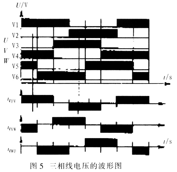
(5) The bridge type three-phase inverter main circuit composed of V1 to V6 is the core circuit of the inverter. Figure 4 is the main circuit diagram of the three-phase inverter, the input terminals are A, B, and the outputs are U, V, W. In the conduction sequence of V1 to V6 in Fig. 5, the shaded portion is the on-time of each IGBT. The time of each cell is π/3, and the waveform of the three-phase line voltage is as shown in Fig. 5.
As seen from Fig. 4, the phase difference between U, V, and W is 2Ï€/3, and the amplitude is equal to the DC voltage Ud. It can be seen that as long as the on and off of the six inverters are controlled in a certain order, the direct current can be inverted into three-phase alternating current.
(6) If the square wave voltage is modulated into a series of pulses according to the sine wave law, even if the duty cycle of the pulse series is arranged in a sinusoidal manner, when the sine value is maximum, the pulse width is the largest; otherwise, when the sine value is the most hour. The width of the pulse is also minimal, and the finer the pulse width is modulated. That is, the more the number of pulses in one cycle, the better the waveform of the output after modulation, the closer the current waveform of the motor load is to the sine wave, and the load waveform is shown in Fig. 6.

3 IGBT protection in DC 600 V power supply system Because IGBT has poor over-voltage and over-current resistance, it will be damaged in case of accident, so IGBT must be protected. IGBT of passenger car DC 600 V power supply system inverter The module has overvoltage, undervoltage protection, overcurrent, overload, overheating and other protection functions.
3.1 Overvoltage and undervoltage protection.
When using IGBT as a switch. Due to the sudden change in the current of the main network, it is easy to generate a high DC voltage and a surge spike voltage when applied to the IGBT collector-emission. The generation of DC overvoltage is caused by an abnormality in the input of the input AC or IGBT. The solution is to derate the IGBT when selecting the IGBT; it can also break the input of the IGBT and the safety of the IGBT when detecting the overvoltage of m. At present, the measures taken against the surge voltage are:
(1) When the operating current is large, in order to reduce the turn-off overvoltage, the wiring inductance of the main circuit should be minimized as much as possible;
(2) Set the RCD snubber circuit as shown in Figure 7 to absorb the protection network. The added snubber diode increases the snubber resistance and avoids the problem of IGBT function being blocked during conduction.
For the output undervoltage caused by the fluctuation of the contact network voltage, the inverter can not stop working, but adopt the method of down-converting, that is, when the input voltage is lower than 540 V, the inverter follows Y/F. =C (constant) law reduces the frequency of the buck operation.
3.2 Over-current and overload protection The IGBT module inverter of the air-conditioned passenger car has the ability to withstand the sudden increase and decrease of the motor load: when the output side and the load are short-circuited, the inverter can immediately block the pulse output and stop working. The IGBT generates overcurrent due to transistor or diode damage, misoperation caused by control or drive circuit failure or interference, output line connection fault or insulation damage, short circuit, short-circuit of the bridge arm of the inverter bridge. The IGBT is subjected to overcurrent for only a few microseconds. The overcurrent protection measures that are usually taken are soft turn-off and reduced gate voltage.
The soft turn-off anti-interference ability is poor. Once the over-current and short-circuit signals are detected, it is turned off, and it is easy to malfunction. The protection circuit is often activated and the device is still damaged. Lowering the gate voltage is to immediately lower the gate voltage to a certain level when the overcurrent signal of the device is detected. At this time, the device remains on, so that the overcurrent value cannot reach the maximum short-circuit peak, and the IGBT can be avoided. The lock is broken. If the fault signal still exists after the delay, the device is turned off; if the fault signal disappears, the drive circuit can automatically resume normal operation. Greatly enhanced anti-interference ability.
When the output of the inverter exceeds its own output capability, called overload, the overload detection of the inverter is based on the current sensor on the output side or the DC current sensor on the input side. In general, the overload protection of the inverter is an inverse time characteristic. That is, the overload current is set to 1.5 times of the rated current for 1 min and then the protection, while less than 1.5 times can extend the protection action time. Above 1.5 times, the protection action is less than 1 min.
3.3 Overheat protection When the temperature of the radiator of the inverter exceeds the allowable temperature, the thermal protection relay of the radiator gives a signal to let the control circuit of the inverter automatically block the pulse and stop working. Generally, the current flowing through the IGBT is large, and the switching frequency is high, so the loss of the device is large. If the heat cannot be dissipated in time, the junction temperature of the device will exceed the maximum value of 125 °C, and the IGBT may be damaged. The heat dissipation is generally a heat sink for forced cooling. In practical applications, a combination of a common radiator and forced cooling is used. A temperature switch is mounted on the heat sink, and a temperature relay can be installed near the IGBT to detect the operating temperature of the IGBT. At the same time, the control actuator cuts off the input of the IGBT when an abnormality occurs to protect its safety.
4 Conclusion IGBT module switch has the advantages of low loss, easy to assemble module structure and uniform switch conversion. It has been increasingly used in railway passenger car power supply systems. When applying IGBT, effective protection measures should be taken for overcurrent, overvoltage and overheating according to actual conditions to ensure safe and reliable operation of IGBT.
In the vehicle weighing system, if the vehicle has two front and rear axles, Figure 2 is a block diagram of the vehicle weighing system. The front and rear sensors convert the load change into a capacitance change; the capacitance measuring circuit converts the capacitance value into a voltage value; the DSP adds and converts the voltage value output by the sensor, and after the data is calculated and processed, the vehicle load value is sent to the display. Due to the large amount of data to be collected in the system, especially the dynamic weighing measurement, in order to meet the real-time requirements of the system, the vehicle weighing acquisition system uses AD7891 and TMS320LF2407 DSP to realize vehicle weighing data acquisition.
3 system hardware design system uses the AD7891 A/D converter of Analog Devices, Inc., which is a 12-bit data acquisition system (DAS) with input multiplexer and sample-and-hold amplifier. The input analog signal range is -10. ~+10 V, theoretical accuracy index up to 4.88 mV, suitable for connection with various microprocessors, controllers and digital signal processors. It has two parallel and serial modes of operation with the DSP, and has eight analog signal channels with overvoltage protection, allowing an overvoltage value of ±17 V. When sampling only one channel signal, the maximum sampling rate is up to 454. .5 kS/s. The AD7891 operates from a single supply and consumes low power. Ideal for applications such as data acquisition systems and test equipment. Therefore, the vehicle weighing system uses the AD7891 to fully meet the system requirements. In the high-speed acquisition system, the AD7891 and DSP are usually combined in serial or parallel mode, and the software controls the data line to achieve the required acquisition speed. The AD7891 and DSP use parallel mode to implement timing control of the AD7891 using A, B, C, D, and E data and direction controllers on the DSPI/O port. In addition, since the I/O port voltage of the DSP is 3.3 V, and the port voltage of the AD7-891 is 5 V, when the port of the DSP only sends a signal to the port of the AD7891. It is directly connected to the AD7891 through the I/O port of the DSP; however, if the signal is sent directly from the port of the AD7891 to the port of the DSP, the DSP may be damaged. Therefore, a high-speed bidirectional level shifter is required. Here, P174LVCC424-5A is selected. Since one P174LVCC4245A can only process 8-bit data lines, two P174LVCC4245A are required for level matching. Its hardware connection circuit is shown in Figure 3. In Figure 3, DSP is pair A. The timing control of the D7891 is completely realized by the I/O port of the TMS320LF2407 DSP, and D[O:11] points to the DSP interface. The CS, WR, CONVST, RD, and EOC timing control pins of the AD7891 match the IOPB4, IOPB5, IOPB6, IOPB7, and IOPF4 of the DSP I/O port, respectively. The AD7891 pin and the DSP I/O port are connected through a 2-level level shifter P174LVCC4245A. The pin configuration is shown in Figure 3.
4 system software design The system program flow is mainly to analyze the error of the collected data. Figure 4 shows the flow of the vehicle weighing data processing program. The DSP, AD7891 and peripheral components are initialized, including setting the stack pointer, setting the timer working mode and enabling it to interrupt, setting the initial value of the data memory and initializing the A/D converter. After the system is powered on, the initialization procedure is first executed. After the initialization is complete. The signal acquisition and A/D conversion programs are called to separately collect the capacitive sensor output signals of the front and rear axles and the vehicle acceleration sensor output signals.
Seen in Figure 4. The key to the program is to accurately capture the sensor output voltage. In order to achieve high-speed sampling of the vehicle weighing system, the timing of the AD7891 is first analyzed. Figure 5 shows the parallel operation timing of the AD7891.
In Figure 5, t1 is the trigger time from CS to RD/WR, t2 is the write pulse width, not less than 35 ns; t3 is the write valid data time, not less than 25 ns; t4 is the effective data retention time, not less than 5 ns ;t5 is the hold time of CS to RD/WR, t6 is the CONVST pulse width time, not less than 35 ns; t7 is the EOC pulse width time, not less than 55 ns; t8 is the degree pulse width, not less than 35 ns; t9 is RD The data read time after the falling edge is not less than 25 ns; tCONV is the conversion time, not more than 1.6μs. In order to achieve high-speed real-time sampling of the measurement and control system, the above time must be accurately and accurately allocated. The working sequence of the AD7891 is realized by the I/O port of the DSP. The system DSP clocked at 30 MHz with a divided 15 MHz output and a single-cycle instruction running for 33 ns. Execute an I/O port instruction in C language. After compiling, it takes about 4 cycles of instruction time. The following is the C language program code collected by the measurement and control system DSP for channel 1:
The above program code can completely control the AD7891 timing shown in Figure 5, so as to meet the accuracy, real-time and high-speed requirements of the vehicle weighing system for the acquisition system.
5 Test results The vehicle weighing system test was carried out on a light goods vehicle with a rated load of 500 kg. During the test, the cab was used for 2 people and weighed a total of 75kg. The sandbag was evenly placed on the front of the compartment as a load, and the speed was up to 40 km/h. Figure 6 records the change in the output voltage of the vehicle during the entire process of acceleration, braking, and stop. In Fig. 6, the time period: 0~9 s is the engine stalling and ignition phase. At this time, the output voltages of the front and rear axles are unchanged: 9~18 s is the acceleration start phase of the gear, and the acceleration is obviously increased. The output voltage of the front axle sensor is reduced, and the output voltage of the rear axle sensor is increased. In the subsequent 18~32 s phase, including the shifting and acceleration process, the vehicle is coasting during the shifting, the acceleration is reduced, and the output voltage of the front axle is increased. The output voltage of the rear axle decreases; from the 32nd s to the off-shift phase, the braking starts, the acceleration decreases sharply, the output voltage of the front axle increases significantly, the output voltage of the rear axle decreases, and the maximum peak point is reached at the 38th s. The test results prove that the system design can complete the system's demand for high-speed real-time data acquisition.
6 Conclusion The vehicle weighing acquisition system uses the I/O port of the DSP to read the data of the AD7891. Full control of the timing of the AD7891 by programming the DSP, while occupying a large number of DSP I/O ports. However, due to the rich I/O port of the TMS320LF2407 DSP, this implementation is completely feasible. The device has the advantages of simple structure and low cost, and can not only meet the static weighing of the vehicle, but also the accuracy of the dynamic weighing is higher than 2%, which can fully meet the requirements of highway overload detection.
Ferrite Magnet,Ferrite Core Magnet,Permanent Ferrite Magnet
Ningbo Wewinmagnet Co.,Ltd , http://www.wewinmagnet.com