The introduction is to completely eliminate the overload phenomenon, prohibit overloaded vehicles from getting on the road, and realize that the driver can know the load of the vehicle in the cab, and the ground inspectors can detect the load of the vehicle at any time and any place through the wireless communication device, thereby helping to stop the overload behavior of the vehicle. . Therefore, a design scheme of vehicle weighing acquisition system based on AD7891 is proposed here. The system design uses a capacitive method to detect vehicle loads and uses the vehicle's own leaf spring as the elastomer for the load cell.
This article refers to the address: http://
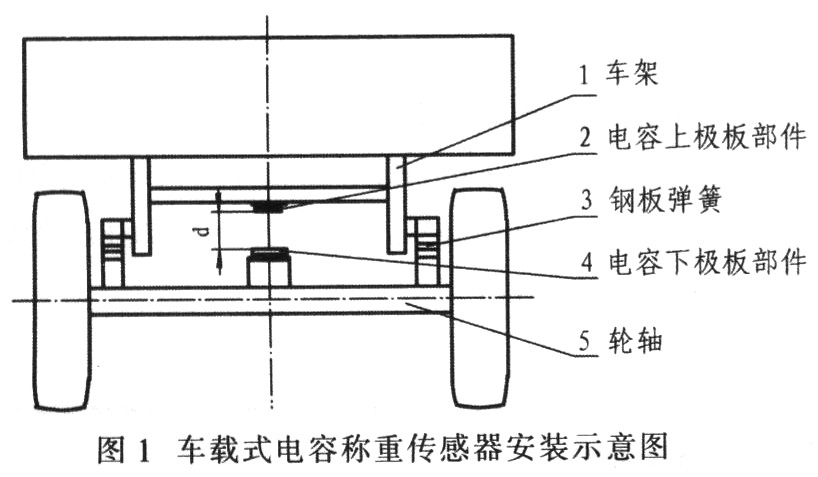
2 Introduction to Vehicle Weighing System Vehicle capacitive weighing device is installed on the vehicle under test. The core device of the weighing device is a capacitive load cell. The plate of the capacitive sensor is installed between the middle of the vehicle axle and the bottom of the vehicle (or the frame). By measuring the deformation of the vehicle leaf spring, the change of the capacitance value is obtained. Load value. Figure 1 is a schematic diagram of a vehicle-mounted capacitive load cell.
In the vehicle weighing system, if the vehicle has two front and rear axles, Figure 2 is a block diagram of the vehicle weighing system. The front and rear sensors convert the load change into a capacitance change; the capacitance measuring circuit converts the capacitance value into a voltage value; the DSP adds and converts the voltage value output by the sensor, and after the data is calculated and processed, the vehicle load value is sent to the display. Due to the large amount of data to be collected in the system, especially the dynamic weighing measurement, in order to meet the real-time requirements of the system, the vehicle weighing acquisition system uses AD7891 and TMS320LF2407 DSP to realize vehicle weighing data acquisition.

3 system hardware design system uses the AD7891 A/D converter of Analog Devices, Inc., which is a 12-bit data acquisition system (DAS) with input multiplexer and sample-and-hold amplifier. The input analog signal range is -10. ~+10 V, theoretical accuracy index up to 4.88 mV, suitable for connection with various microprocessors, controllers and digital signal processors. It has two parallel and serial modes of operation with the DSP, and has eight analog signal channels with overvoltage protection, allowing an overvoltage value of ±17 V. When sampling only one channel signal, the maximum sampling rate is up to 454. .5 kS/s. The AD7891 operates from a single supply and consumes low power. Ideal for applications such as data acquisition systems and test equipment. Therefore, the vehicle weighing system uses the AD7891 to fully meet the system requirements. In the high-speed acquisition system, the AD7891 and DSP are usually combined in serial or parallel mode, and the software controls the data line to achieve the required acquisition speed. The AD7891 and DSP use parallel mode to implement timing control of the AD7891 using A, B, C, D, and E data and direction controllers on the DSPI/O port. In addition, since the I/O port voltage of the DSP is 3.3 V, and the port voltage of the AD7-891 is 5 V, when the port of the DSP only sends a signal to the port of the AD7891. It is directly connected to the AD7891 through the I/O port of the DSP; however, if the signal is sent directly from the port of the AD7891 to the port of the DSP, the DSP may be damaged. Therefore, a high-speed bidirectional level shifter is required. Here, P174LVCC424-5A is selected. Since one P174LVCC4245A can only process 8-bit data lines, two P174LVCC4245A are required for level matching. Its hardware connection circuit is shown in Figure 3. In Figure 3, DSP is pair A. The timing control of the D7891 is completely realized by the I/O port of the TMS320LF2407 DSP, and D[O:11] points to the DSP interface. The CS, WR, CONVST, RD, and EOC timing control pins of the AD7891 match the IOPB4, IOPB5, IOPB6, IOPB7, and IOPF4 of the DSP I/O port, respectively. The AD7891 pin and the DSP I/O port are connected through a 2-level level shifter P174LVCC4245A. The pin configuration is shown in Figure 3.

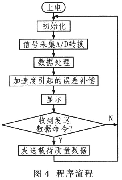
4 system software design The system program flow is mainly to analyze the error of the collected data. Figure 4 shows the flow of the vehicle weighing data processing program. The DSP, AD7891 and peripheral components are initialized, including setting the stack pointer, setting the timer working mode and enabling it to interrupt, setting the initial value of the data memory and initializing the A/D converter. After the system is powered on, the initialization procedure is first executed. After the initialization is complete. The signal acquisition and A/D conversion programs are called to separately collect the capacitive sensor output signals of the front and rear axles and the vehicle acceleration sensor output signals.
Seen in Figure 4. The key to the program is to accurately capture the sensor output voltage. In order to achieve high-speed sampling of the vehicle weighing system, the timing of the AD7891 is first analyzed. Figure 5 shows the parallel operation timing of the AD7891.
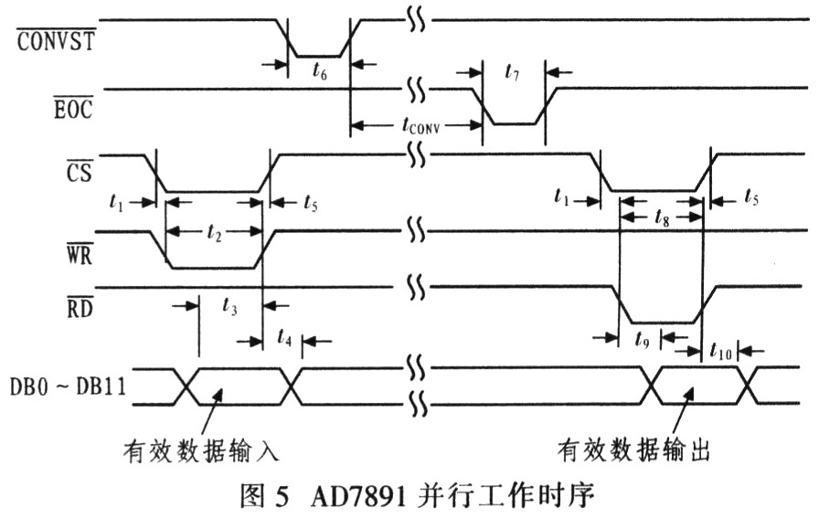
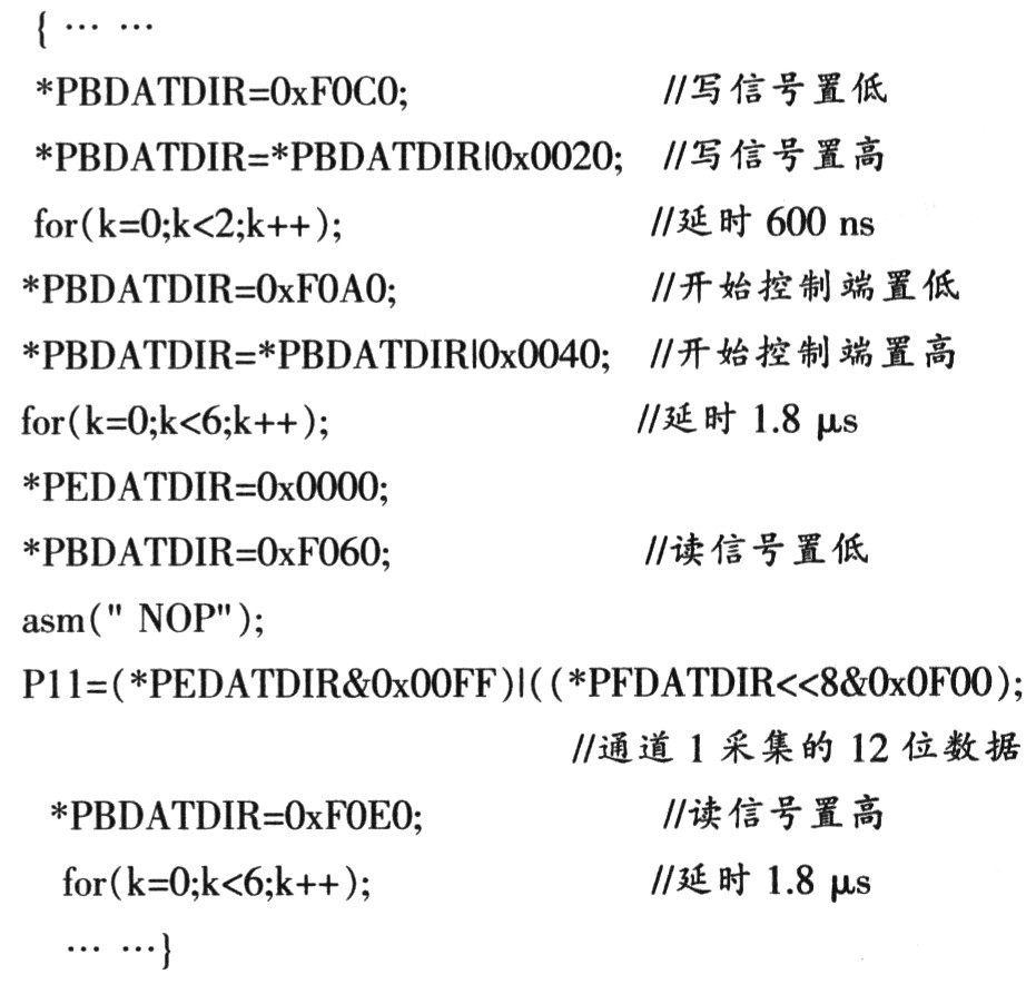
In Figure 5, t1 is the trigger time from CS to RD/WR, t2 is the write pulse width, not less than 35 ns; t3 is the write valid data time, not less than 25 ns; t4 is the effective data retention time, not less than 5 ns ;t5 is the hold time of CS to RD/WR, t6 is the CONVST pulse width time, not less than 35 ns; t7 is the EOC pulse width time, not less than 55 ns; t8 is the degree pulse width, not less than 35 ns; t9 is RD The data read time after the falling edge is not less than 25 ns; tCONV is the conversion time, not more than 1.6μs. In order to achieve high-speed real-time sampling of the measurement and control system, the above time must be accurately and accurately allocated. The working sequence of the AD7891 is realized by the I/O port of the DSP. The system DSP clocked at 30 MHz with a divided 15 MHz output and a single-cycle instruction running for 33 ns. Execute an I/O port instruction in C language. After compiling, it takes about 4 cycles of instruction time. The following is the C language program code collected by the measurement and control system DSP for channel 1:

6 Conclusion The vehicle weighing acquisition system uses the I/O port of the DSP to read the data of the AD7891. Full control of the timing of the AD7891 by programming the DSP, while occupying a large number of DSP I/O ports. However, due to the rich I/O port of the TMS320LF2407 DSP, this implementation is completely feasible. The device has the advantages of simple structure and low cost, and can not only meet the static weighing of the vehicle, but also the accuracy of the dynamic weighing is higher than 2%, which can fully meet the requirements of highway overload detection.
Energy Saving Lights ,Fluorescent Light Bulbs ,Energy Saving Lamps
f.s.c. Technology Corp., Limited , http://www.cfl-manufacturer.com