1 switching power supply circuit design
The switching power supply circuit in the system provides a stable voltage for charging the battery. A flyback switching power supply circuit is used. The circuit of the flyback switching power supply is relatively simple, using a large energy storage filter inductor and a freewheeling diode less than the forward switching power supply. Therefore, the size of the flyback switching power supply is larger than that of the forward switching power supply. Small size and low cost. In addition, the output voltage of the flyback switching power supply is modulated by the duty cycle, which is much higher than that of the forward switching power supply. Therefore, the flyback switching power supply requires a lower error signal amplitude for adjusting the duty cycle. The gain and dynamic range of the signal amplifier are also small. Based on these advantages, flyback switching power supplies are widely used in the field of home appliances. as shown in picture 2.
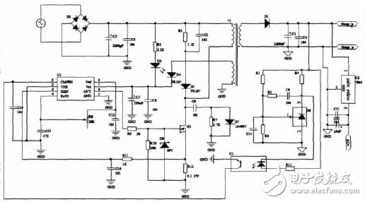
Figure 2 switching power supply circuit
The switching power supply circuit control chip adopts UC3842, and UC3842 is an ideal new pulse width modulator. The switching regulator power supply composed of the integrated circuit has the following characteristics compared with the voltage controlled pulse width modulation switching power supply:
1) Fine-tuning the oscillator discharge current to precisely control the duty cycle;
2) The current mode operates to 500 kHz;
3) Automatic feedforward compensation;
4) Latch pulse width modulation, which can be limited by cycle;
5) Internally trimmed reference voltage with undervoltage lockout;
6) High current totem pole output;
7) Undervoltage lockout with hysteresis;
8) Low startup and operating current.
The TL431 is called an adjustable precision shunt regulator. It can be used to set any reference voltage in the range of 2.5V~36V with two external resistors. The working principle is that when the output voltage U 0 fluctuates, the sampling voltage obtained by the voltage divider is compared with the 2.5V bandgap reference voltage in the TL431, and an error voltage is formed at the cathode to make the operating current of the LED corresponding. Change, and then through the optocoupler to change the size of the control terminal current Ic, adjust the output duty cycle of the switch tube, so that the output voltage U0 does not change, thereby achieving the purpose of voltage regulation.
2 charge and discharge circuit design
The charge and discharge process in this design is mainly done by two P-channel field effect transistors IRF9540N. As shown in Figure 3. The Q2 tube controls the charging process of the system, while the discharge pulse is mainly controlled by Q3.
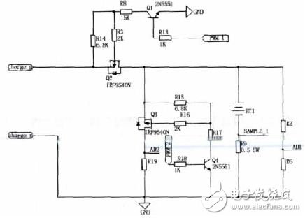
Figure 3 charging and discharging circuit diagram
3 acquisition part
There is a 12-bit precision AD conversion module ADC12 in the MSP430F149. The ADC 12 can convert one of eight external analog signals or one of four internal voltages. The ADC core converts the analog signal into 12-bit data and stores it in a conversion memory register. The core uses two reference levels, VR+ and VR-, as the upper and lower limits of the conversion range and the range value of the reading and the "0" value. The conversion value is full scale when the input signal is greater than or equal to VR+, and is “0†when it is less than or equal to VR-. The battery terminal voltage is divided by two resistors R2 and R6 to limit the sampling voltage value AD1 of the single chip to the input voltage range. Both the charging current and the discharging current are converted into corresponding voltage values ​​through the resistors and sent to the AI ​​port of the microcontroller. The three AD samples are stored in the corresponding ADC12MEMx registers.
4 drive section
According to the three-way AD sampling result to determine the charging state of the charger, the PWM waveforms PWM1 and PWM2 with two channels of duty cycle adjustable frequency of 1 kHz are output by the single-chip microcomputer to control the conduction degree of the two transistors 2N5551, and the collector current of the triode Depending on the difference, the resistors are divided to provide different voltages to the gate of the FET, drive the MOSFET, output the drain current Id of constant size, and provide the battery with different charging currents and discharge pulse amplitudes. Finally, the effect of pulse charging is achieved.
Beverage Refrigerator,Drink Refrigerator,Cold Drink Refrigerator,Commercial Beverage Refrigerator
ZHENGZHOU KAIXUE COLD CHAIN CO., LTD. , https://www.supersnowfreezer.com