ESD protection is important for high density, miniaturization and complex electronic devices. This paper discusses the effects of parameters such as minimum breakdown voltage and breakdown current, maximum reverse leakage current and rated reverse shutdown voltage on the circuit when using TVS diodes to prevent ESD, and for portable consumer electronic devices, set-top boxes, As well as video line protection, USB protection and RJ-45 interface in personal computers, some typical applications are introduced.
With the rapid development of products such as mobile products, printers, PCs, DVDs, and set-top boxes (STBs), consumers are demanding more and more advanced performance. Semiconductor components are increasingly becoming smaller, denser, and more complex, especially for applications such as fashion consumer electronics and portable products that are critical to motherboard area and are susceptible to electrostatic discharge. Some complex semiconductor functional circuits that use deep submicron processes and very fine linewidth routing are more sensitive to the effects of circuit transients and will cause these problems to be exacerbated.
ESD protection principleThere are several techniques for circuit protection components. When selecting circuit protection components, if the designer chooses improper protection devices, it will only provide the wrong security concept. The choice of circuit protection components should be based on the wiring conditions to be protected, the available board space, and the electrical characteristics of the circuit being protected. In addition, it is necessary to know the characteristics of the protection components. One of the important factors to consider is the clamping voltage of the device. The so-called clamp voltage is the voltage across the transient voltage canceller (TVS) in the ESD device, which is the strain voltage of the protected IC.
Because the oxide layer is thinner in IC circuits fabricated using advanced process technology, the gate oxide layer is more susceptible to damage. This means that a higher clamping voltage will produce a higher strain voltage on the protected IC device and increase the probability of failure.
Many protection components are designed to absorb a large amount of energy, which also results in a high clamping voltage due to component structure or design. Since the varistor clamp voltage is too high, they are not able to provide effective ESD protection. In addition, they cannot provide protection for high speed data lines due to the high capacitance of the varistor. TVS diodes have been created to solve this problem, and it has become a key technology to protect portable electronic devices.
TVS diodes are solid-state components specifically designed to absorb ESD energy and protect the system from ESD damage. If properly applied, the TVS diode will limit the voltage across the protected device just above the rated operating voltage, but well below the breakdown threshold voltage.
TVS related parametersThe best way to handle transient damage to the device is to direct the instantaneous current away from the sensitive device. The TVS diode is connected in parallel with the protected line on the circuit board. When the instantaneous voltage exceeds the normal operating voltage of the circuit, the TVS diode is avalanche, providing an ultra-low resistance path to the instantaneous current. As a result, the instantaneous current is diverted through the diode. The protected device is turned on and the protected circuit is kept at the off voltage until the voltage returns to normal. When the instantaneous pulse is over, the TVS diode automatically returns to the high-impedance state, and the entire loop enters the normal voltage. Many devices degrade their parameters and performance after being subjected to multiple shocks, and the diodes will not be damaged or degraded as long as they operate within a limited range.

As can be seen from the above process, when selecting a TVS diode, you must pay attention to the following parameters:
1. Minimum breakdown voltage VBR and breakdown current IR. VBR is the minimum breakdown voltage of TVS. At 25 ° C, below this voltage TVS will not avalanche. When the TVS flows through a prescribed 1 mA current (IR), the voltage applied to the two poles of the TVS is its minimum breakdown voltage VBR. According to the degree of dispersion of TVS VBR and standard values, VBR can be divided into 5% and 10%. For 5% of VBR, VWM = 0.85 VBR; for 10% of VBR, VWM = 0.81 VBR. In order to meet the IEC61000-4-2 international standard, TVS diodes must meet the test standards for IEC61000-4-2 ESD protection level 4, minimum 8kV (contact) and 15kV (air) ESD impact, Thunder Electronics in automotive electronics The TVS device can meet the contact and air 30KV test, so for some applications with special requirements, the designer can select the device as needed.
2. Maximum reverse leakage current ID and rated reverse shutdown voltage VWM. VWM This is the voltage that the diode can withstand in the normal state. This voltage should be greater than or equal to the normal working voltage of the protected circuit. Otherwise, the diode will continuously cut off the loop voltage; but it needs to be as close as possible to the normal working voltage of the protected loop. This will not cause the entire loop to face an overvoltage threat before the TVS works. When this rated reverse turn-off voltage VWM is applied between the two poles of the TVS, it is in the reverse-off state, and the current flowing through it should be less than or equal to its maximum reverse leakage current ID.
3. Maximum clamp voltage VC and maximum peak pulse current IPP. When the pulse peak current IPP with a duration of 20 mS flows through the TVS, the maximum peak voltage appearing at both ends thereof is VC. VC and IPP reflect the surge suppression capability of TVS. The ratio of VC to VBR is called the clamping factor and is generally between 1.2 and 1.4. VC is the voltage supplied by the diode in the off state, that is, the voltage passing through the TVS in the ESD strike state. It cannot be greater than the endurable limit voltage of the protected circuit, otherwise the device is in danger of being damaged.
4. Pppm rated pulse power, which is based on the maximum cutoff voltage and the peak pulse current at this time. For handheld devices, a 500W TVS is generally sufficient. The maximum peak pulse power consumption PM is the maximum peak pulse power consumption value that the TVS can withstand. At a given maximum clamping voltage, the greater the power consumption PM, the greater the surge current capability. At a given power consumption PM, the lower the clamp voltage VC, the greater the surge current capability. In addition, peak pulse power consumption is also related to pulse waveform, duration, and ambient temperature. Moreover, the transient pulses that the TVS can withstand are not repeated, and the pulse repetition frequency (ratio of duration to pause time) specified by the device is 0.01%. If repetitive pulses occur in the circuit, the accumulation of pulse power should be considered, possibly damaging the TVS.
5. Capacitance C. Capacitance C is determined by the TVS avalanche junction profile and is measured at a specific 1 MHz frequency. The size of C is proportional to the current carrying capacity of the TVS, and C is too large to attenuate the signal. Therefore, C is an important parameter for the TVS of the data interface circuit. Capacitance For loops with higher data/signal frequencies, the greater the interference of the diode's capacitance on the circuit, the more noise is formed or the signal strength is attenuated. Therefore, the capacitance range of the selected device needs to be determined according to the characteristics of the loop. Generally, the high-frequency circuit should be chosen to have a small capacitance (such as LCTVS, low-capacitance TVS, and a capacitance of no more than 3pF), while the circuit capacitance that requires less capacitance can be higher than 40pF.
ESD application 1. Application of bottom connectorThe bottom connector design is widely used in mobile consumer products. Currently, the products on the market are mainly mobile phones, PDAs, DSCs (digital cameras) and portable products such as MP3.
Since it is a DC circuit, a common capacitor device can be used. This port can be subject to high energy shocks, with optional TVS or discrete devices.
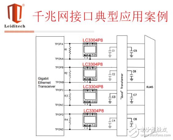
The RJ-45 interface is widely used in network-connected interface devices. A typical application is a 10/100/1000M Ethernet network.

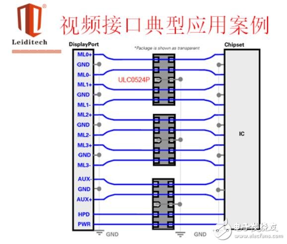
The current video output ports are designed with D-SUB, DVI (28 lines), SCART (19 lines) and D-TERMINAL (mainly for Japanese products). The video data line has a high data transmission rate, the data transmission rate is as high as 480 Mbps, and some video data transmission rates reach 1 G or more. Therefore, a low capacitance TVS is selected, which usually connects a low capacitance diode in series with the TVS diode to reduce the entire line. Capacitors (less than 3pF) meet the requirements of high-rate loops. Shanghai Thunder Electronics' ULC0524P has good low-capacitance characteristics and can provide 4-way ESD protection, while its successor SRDA05-6 can provide up to 6 ESD protections. The SRDA05-X series is suitable for the protection of all high-speed communication lines.
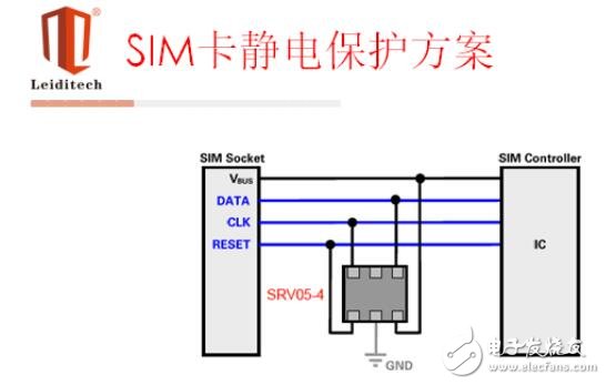
SIM card data line protection has always been the focus of each company's products, and the ESD (TVS) / EMI / RFI protection for one of these ports is designed to protect the chip device's unlimited integration solution.
When selecting devices for different purposes, avoid operating the device near the limits of its design parameters, and select devices with fast enough response and high sensitivity based on the characteristics of the protected circuit and the characteristics that may be subject to ESD strikes. Effectively playing the role of the protection device is critical, and devices that integrate other functions should also be considered first.
Thunder also offers a variety of different TVS diode packages, especially micro packages such as SOT23 and SC-70, and flip-chips of the same size as the chip, which only occupy about 4.8mm2 on the board, but Multiple lines can be protected at the same time. Many new products have recently adapted to the high integration and miniaturization requirements of portable devices. Integrating EMI/RFI/ESD protection into one device not only reduces space, but also greatly reduces costs, reduces device procurement costs and processing. Cost, for the port that needs these kinds of protection functions at the same time, it is the designer's first choice.
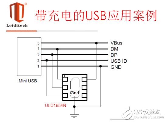
For the increasingly fast charging USB, it is especially important for the surge protection of Vbus. For fast charging USB, there is a corresponding ULC1654N to meet the protection needs.
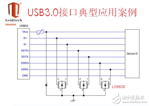
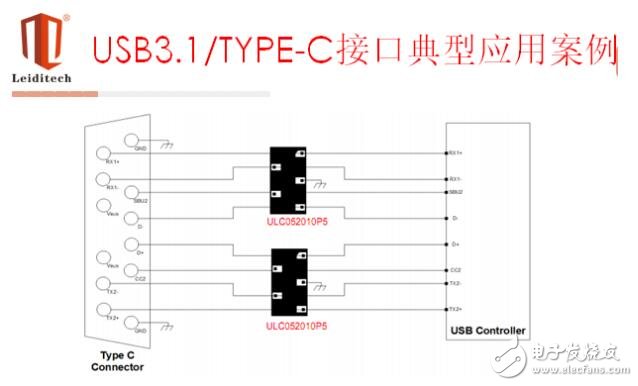
5. USB protection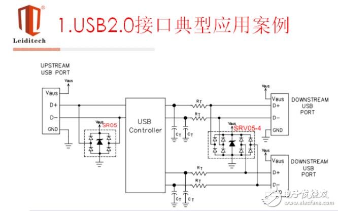
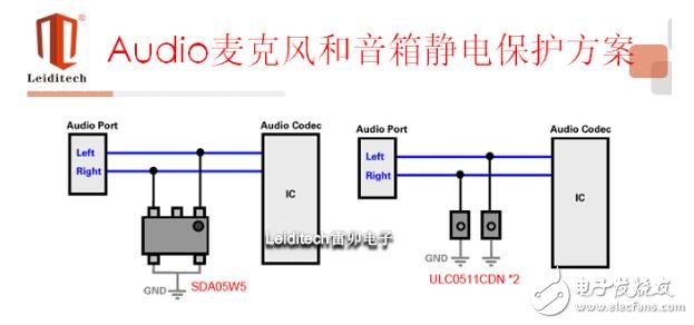
In terms of audio data line protection, because the signal rate of the audio loop is relatively low, the requirements for device capacitance are not too high, and the common capacitance index is acceptable. In some mobile phone designs, the earphone and the microphone are combined together, while others are combined. It is a separate line. In the former case, a single TVS can be selected, and in the latter case, if the two circuits are adjacent, a multi-channel TVS array can be selected, and the protection of the two circuits can be completed with only one device.
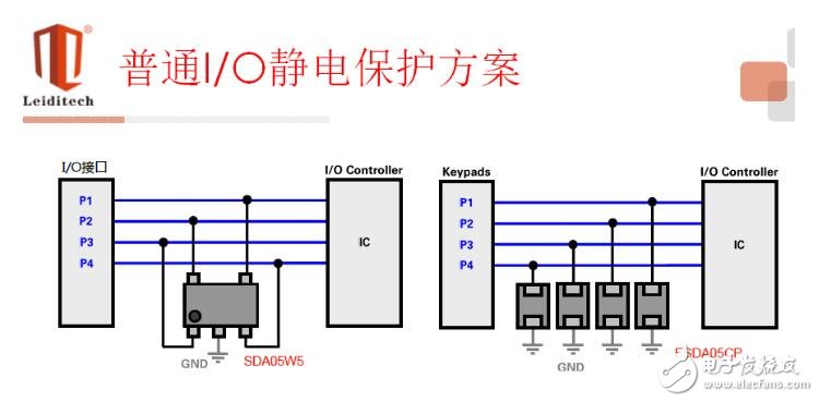
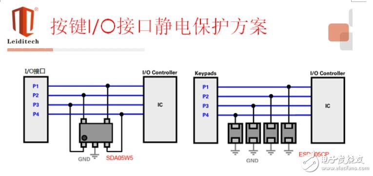
For buttons and switching circuits, the data rate of these circuits is very low, there is no special requirement for the capacitance of the device, and ordinary TVS arrays can be used. The above devices are all used for ESD protection on mobile phones. In fact, they are a 5V anti-static, which can meet the needs of static electricity.
Plug-in Piece Sensor
Feyvan Electronics designs and manufactures NTC temperature sensors, probes, and cable assemblies with excellent long-term stability, high accuracy and short response time in high-temperature sensing applications such as automotive, home appliance and industrial use from -40℃ to +250℃.
With more than 15 years of NTC thermistors and sensor probes production experiences, Feyvan electronics provide various choices for a wide range of applications and are available in custom engineered probe package configurations for a variety of mounting and connectivity options with low costs.
Plug in Sensor,Sensor Coffee Maker,Sensor Coffee Machines,Automotive Sensors
Feyvan Electronics Technology Co., Ltd. , https://www.fv-cable-assembly.com