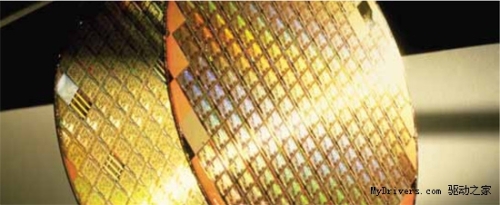
 Samsung Electronics announced today that it has successfully implemented a 20-nm process test chip, which is by far the most advanced semiconductor manufacturing process in the industry.
 Samsung Electronics used an integrated digital flow RTL-to-GDSII provided by Cadence Design Systems, an electronic design automation company in California. This Encounter-based process and method fully meets the complex requirements of Samsung's 20nm test chip from IP integration to design verification, including the Encounter digital deployment system, Encounter RTL compiler, Incisive Enterprise Simulator, Encounter power system, QRC Extraction extraction tool, Encounter timing system, Encounter testing and physical verification system, Encounter NanoRoute routing and so on.
Samsung's test chip consists of an ARM Cortex-M0 microprocessor and ARM Artisan physical IP, but Samsung did not reveal how many transistors were included in the 20nm process and how big the core area was.
It is also known that Samsung's 20nm process will use second-generation Gate Last and high-K metal gate (HKMG) technologies, second-generation ultra-low-K dielectric materials, fifth-generation strained silicon wafers, and 193-mm immersion Photolithography process.
In spite of its success with just tapeout, Samsung's 20nm Early Process Design Kit (PDK) has been opened to customers so that they can begin designing the next generation of new process products.
Samsung and Cadence have previously had in-depth cooperation, including the IBM-led Common Platform (General Platform); the alliance under the 32/28nm process, and low-power HKMG technology and so on.
Instrument Cable ,Thermocouple Extension Wire ,Thermocouple Extension,Instrument Cable Types
Electric Wire & Cable Co., Ltd. , http://www.nbcables.com