This article provides an overview of the basic working principles of diodes, OR gates, and triodes. These components are fundamental in digital electronics and play a key role in logic circuit design.
Diode AND Gate Principle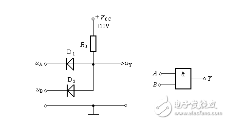
As shown in the diagram, this is a simple diode AND gate circuit with a supply voltage of Vcc = 10V. In this context, a high level is defined as 3V or above, while a low level is considered to be 0.7V or below.
Let’s analyze the circuit under different input conditions:
1. When both Ua and Ub are at 0V, the diodes D1 and D2 are forward-biased and conduct. As a result, the output voltage at point Uy will be approximately 0.7V, which is the typical forward voltage drop of a silicon diode.
2. If one input is high (e.g., Ua = 3V) and the other is low (Ub = 0V), the diode connected to the low input (D2) will conduct, keeping the output at 0.7V. The other diode (D1) will be reverse-biased and thus not conduct, ensuring that the output remains stable at 0.7V.
3. When both inputs are high (Ua = Ub = 3V), both D1 and D2 are forward-biased. However, the output voltage at Uy will be clamped at 3.7V due to the combined effect of the input voltage and the diode's forward voltage drop.
In general, when a diode is conducting, its anode potential is about 0.7V higher than its cathode, and vice versa. This behavior is often referred to as the "clamping" effect of the diode, which helps stabilize voltages in circuits.
Diode OR Gate Principle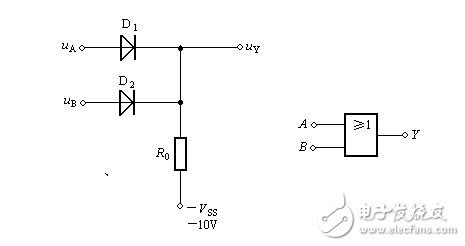
This figure illustrates a basic diode OR gate. Here, Vss is set to 0V instead of -10V for simplicity.
Let’s examine the operation of this circuit:
1. When both Ua and Ub are at 0V, both diodes D1 and D2 are reverse-biased and do not conduct. Therefore, the output voltage at point Uy remains at 0V.
2. If one input is high (e.g., Ua = 3V) and the other is low (Ub = 0V), the corresponding diode (D1) will conduct, allowing current to flow. The output voltage will then be approximately 3V minus the 0.7V diode drop, resulting in 2.3V at Uy.
3. When both inputs are high (Ua = Ub = 3V), both diodes are forward-biased, and the output voltage remains at 2.3V regardless of the number of active inputs.
The OR gate allows the output to be high if at least one input is high, making it a useful component in digital logic systems.
Triode NOT Gate Circuit Principle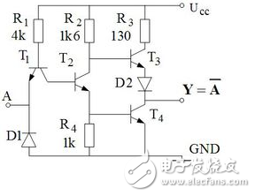
This diagram shows a transistor-based NOT gate. It consists of resistors and transistors arranged to create a switching circuit. The base-emitter junctions of the transistors act like diodes, contributing to the overall voltage division in the circuit.
The circuit includes a 4kΩ resistor connected to the collector junction of T1, followed by the emitter junction of T2, and finally a 1kΩ resistor. Together, these form a series voltage divider that controls the state of the transistors.
Under normal conditions, the base of T1 is always higher than its collector by about 0.7V, and the total forward voltage drop across two PN junctions is around 1.4V. This results in a voltage drop of 3.6V across the resistors. Using the voltage divider formula, the 4kΩ resistor drops approximately 2.9V, leaving the collector voltage of T1 at around 1.4V.
When a high-level signal (above 3.6V) is applied to the A terminal, the T1 collector voltage becomes lower than its emitter, causing current to flow through T1 and into the emitter of T2. This turns T2 on, leading to saturation of T4 and a low output level.
Conversely, when a low-level signal (below 1V) is applied, the emitter of T1 is at a lower voltage than the collector, preventing current from flowing through T1. This keeps T2 off, and T4 also remains off. In this case, the circuit outputs a high level, effectively performing a NOT function.
By understanding how these components interact, we can build more complex digital circuits that perform logical operations essential in modern computing and communication systems.
Switching Power Supply Transformer,High Frequency Switching Power Transformer,High Power High-frequency Transformer,Small electrical transformer
Xuzhou Jiuli Electronics Co., Ltd , https://www.xzjiulielectronic.com