This article provides an overview of the basic principles behind diodes, OR gates, and triodes. These components are fundamental in digital electronics and play a crucial role in building logic circuits.
Diode AND Gate Principle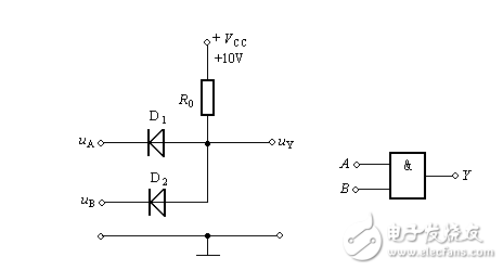
As shown in the diagram, this is a diode-based AND gate circuit with Vcc set to 10 volts. In this setup, any voltage above 3 volts is considered a high level, while anything below 0.7 volts is treated as a low level. Let's take a closer look at how this circuit behaves under different input conditions.
1. When both Ua and Ub are 0 volts, both diodes D1 and D2 are forward-biased and conduct. As a result, the output voltage at point Uy is approximately 0.7 volts, which is the typical forward voltage drop of a silicon diode.
2. If one input is high (e.g., Ua = 3V) and the other is low (Ub = 0V), D2 will be forward-biased and conduct, limiting its voltage drop to 0.7V. At this point, D1 becomes reverse-biased because the right side of D1 is at 0.7V while the left side is at 3V. Thus, the output remains at 0.7V regardless of which diode you start analyzing from.
3. When both inputs are high (Ua = Vb = 3V), both D1 and D2 are forward-biased, and the output voltage is clamped to 3.7 volts. This behavior is consistent with the concept of a "clamping" action of the diode once it is conducting.
In summary, when a diode is conducting, if the cathode potential is fixed, the anode potential is always about 0.7V higher. Conversely, if the anode potential is fixed, the cathode potential is about 0.7V lower. This effect is known as the clamping action of a diode.
Diode OR Gate Principle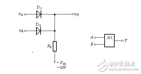
The diagram shows a diode-based OR gate. Here, Vss is set to 0 volts instead of -10 volts for simplicity. Let’s analyze its operation under different input scenarios:
1. When both Ua and Ub are 0 volts, both diodes D1 and D2 are reverse-biased and do not conduct. As a result, the output voltage at point Uy is 0 volts.
2. If one input is high (e.g., Ua = 3V) and the other is low (Ub = 0V), D1 conducts, and the output voltage at Uy becomes 3 - 0.7 = 2.3 volts. Similarly, if Ua = 0V and Ub = 3V, D2 conducts, and the output remains at 2.3 volts.
3. When both inputs are high (Ua = Vb = 3V), both diodes conduct, and the output voltage is still 2.3 volts. This demonstrates that the OR gate outputs a high signal whenever at least one input is high.
Triode NOT Gate Circuit Principle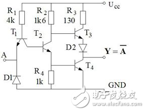
This circuit involves a series of resistors and transistors, forming a voltage divider with two pn junctions. The base of T1 is always 0.7V higher than its collector, due to the forward voltage drop of the pn junction.
The total forward voltage drop across the two pn junctions is 1.4V, leaving 3.6V across the two resistors. Using the voltage divider rule, the 4kΩ resistor drops approximately 2.9V, resulting in a collector voltage of around 1.4V for T1.
When the input A is high (above 3.6V), the emitter voltage of T1 becomes higher than its collector, causing current to flow through T2 and saturating it. This leads to T4 also being saturated, and the output goes low.
Conversely, when the input A is low (below 1V), T1 does not conduct, and no current flows into T2. This causes T2 and T4 to cut off, allowing T3 to saturate and the output to go high. This configuration effectively implements a NOT gate, where the output is the inverse of the input.
Understanding these basic electronic components helps build a solid foundation in digital circuit design and analysis.
High-frequency Transformer,Switching Power Supply Transformer,Ring Electronic Transformer,High Frequency Electrical Transformer
Xuzhou Jiuli Electronics Co., Ltd , https://www.xzjiulielectronic.com