A bridge is an effective way to accurately measure resistance or other analog quantities. This article describes how to interface a silicon strain gage with a large signal output to an analog-to-digital converter (ADC), especially a sigma-delta ADC, which is a low-cost implementation of pressure transmitters when using silicon strain gating. Program
Silicon strain gauge
The advantage of a silicon strain gauge is its high sensitivity, which detects pressure by sensing changes in the body resistance of the silicon material induced by stress. The output is typically an order of magnitude larger than a metal foil or a wire strain gauge. The silicon strain gage has a large output signal and can be used with less expensive electronics. However, the installation and wiring of these small and brittle devices is very difficult, thereby increasing the cost and limiting their use in adhesive strain gage applications.
However, silicon pressure sensors made with MEMS technology have overcome these drawbacks. This MEMS pressure sensor uses standard semiconductor processes and special etching techniques. This special etching technique selectively removes a portion of the silicon from the backside of the wafer to create hundreds of square films surrounded by a solid silicon bezel. On the front side of the wafer, a varistor is implanted on each side of each small film, and the four resistors around the small piece are connected by a metal wire to form a Wheatstone bridge. Finally, use a diamond saw to saw each sensor from the wafer. At this time, the silicon sensor has begun to take shape, but it also needs to be equipped with a pressure port and a connection lead. These small sensors are inexpensive and relatively reliable, but are greatly affected by temperature changes, and the initial offset and sensitivity vary widely.
Pressure sensor example
An example of a pressure sensor is given here, the principles involved of which apply to any sensor that uses a similar bridge. Equation 1 gives an output model of the original pressure sensor. Among them, VOUT has a wide range of variation under a given pressure P, different sensors at the same temperature, or the same sensor at different temperatures, the VOUT is different. Therefore, to provide a consistent, meaningful output, each sensor must be calibrated to compensate for differences and temperature drift between devices. Calibration has long been performed through analog circuits. However, advances in modern electronics have made digital calibration more cost-effective than analog calibration, and their accuracy is better. In addition, with some analog technology tricks, digital calibration can be simplified without sacrificing accuracy.
VOUT=VB(PS0(1+S1(T-T0))+U0+U1(T-T0)) (1)
Where VOUT is the bridge output, VB is the excitation voltage of the bridge, P is the applied pressure, T0 is the reference temperature, S0 is the sensitivity at T0 temperature, S1 is the temperature coefficient of sensitivity (TCS), U0 is in no pressure In the case of the bridge, the output offset (or imbalance) at temperature T0, and U1 is the temperature coefficient of the offset (OTC). Equation (1) uses a one-time multinomial formula to model the sensor, while some applications may use higher-order polynomial formulas, piecewise linear techniques, or piecewise quadratic approximation models, and establish a search for the coefficients therein. table. Regardless of which model is used, digital calibration is performed by digitizing VOUT, VB, and T, and a square formula is used to determine all coefficients and perform the necessary calculations. Equation (2) is derived from the variation of equation (1), from which it can be clearly seen that the information required for the accurate pressure value is output by digital calculation (usually performed by a microcontroller (MCU)).
P=(VOUT/VB-U0-U1(T-T0))/(S0(1+S1(T-T0)) (2)
Voltage driven
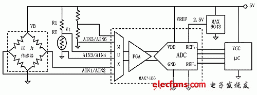
Figure 1 This circuit directly measures the variables required to calculate the actual pressure (excitation voltage, temperature, and bridge output)
In the circuit shown in Figure 1, a high-precision ADC digitizes VOUT (AIN1/AIN2), temperature (AIN3/AIN4), and VB (AIN5/AIN6), which are then passed to the MCU where it is converted. In actual pressure. The bridge is powered directly from the power supply, which also powers the ADC, voltage reference, and MCU. Resistance Formula The temperature detector Rt is used to measure temperature. The input multiplexer in the ADC measures the bridge, RTD, and supply voltage simultaneously. To determine the calibration factor, the entire system (or at least the RTD and bridge) is placed in an incubator and measured at multiple different temperatures. The measurement data is processed by the test system to determine the calibration coefficients, and the final coefficients are downloaded to the MCU and stored in non-volatile memory.
The main consideration when designing this circuit is the dynamic range and resolution of the ADC. The minimum requirements depend on the specific application and the parameters of the selected sensor and RTD. In this example, the specific parameters of the sensor are as follows.
System specification
· Full scale pressure: 100psi
· Pressure resolution: 0.05psi
· Temperature range: -40 to +85 ° C
· Power supply voltage: 4.75 ~ 5.25V
Pressure sensor specifications
· S0 (sensitivity): 150 ~ 300μV / V / psi
· S1 (temperature coefficient of sensitivity): maximum is -2500&TImes; 10-6/°C
· U0 (offset): -3 to +3mV/V
· U1 (temperature coefficient of offset): -15~+15μV/V/°C
· RB (input resistance): 4.5kΩ
· TCR (temperature coefficient of resistance): 1200&TImes; 10-6/°C
· RTD: PT100
o α: 3850&TImes; 10-6/°C
o -40 ° C resistance: 84.27 Ω
o Resistance at 0 °C: 100Ω
o Resistance at 85 °C: 132.80Ω
Voltage resolution
The minimum voltage resolution that the ADC can accept is based on the VOUT corresponding to the minimum pressure change that the sensor can detect. The extreme case is to use the lowest sensitivity sensor to measure at the highest temperature and lowest supply voltage. Note that the offset term in equation (1) does not affect the resolution because the resolution is only related to the pressure response. Using equation (1) and the above assumptions:
VOUTmin=4.75V&TImes; (0.05psi/count×150μV/V/psi×(1+(-2500×10-6/°C)×(85°C-25°C))
≈30.3μV/count
Therefore, the minimum ADC voltage resolution is 30μV/count.
ADC input range
The input range of the ADC depends on the maximum input voltage and minimum voltage. According to Equation 1, the conditions for the maximum VOUT are generated: maximum pressure 100 psi, minimum temperature - 40 ° C, maximum supply voltage 5.25 V and 3 mV/V offset, -15 μV/V/°C offset temperature coefficient, -2500×10- TCS at 6/°C and highest sensitivity at 300μV/V/psi. The minimum signal is typically present without pressure (P = 0), with a supply voltage of 5.25V, an offset of -3mV/V, a temperature of -40°C, and an OTC equal to +15μV/V/°C.
Use equation (1) again and the above assumptions:
VOUTmax=5.25V×(100psi×300μV/V/psi×(1+(-2500×10-6/°C)×(-40°C-25°C))+3mV/V+(-0.015mV/V/°C) ×(-40°C-25°C))=204mV
VOUTmin = 5.25 × (-3mV/V + (0.015mV/V/°C×(-40°C-25°C)))=-21mV
Therefore, the input range of the ADC is -21 to +204 mV.
Resolution
ADCs suitable for this application should have an input range of -21 to +204 mV and a voltage resolution of 30 μV/count. The total number of codes for this ADC is (204mV + 21mV) / (30μV / count) = 7500, and the dynamic range is slightly lower than 13 bits. If the output range of the sensor exactly matches the input range of the ADC, a 13-bit converter will suffice. Since the range of -21 to +204 mV does not match the normal ADC input range, either the input signal is level shifted and amplified, or a higher resolution ADC is selected. Fortunately, current sigma-delta converters have high resolution, with bipolar inputs and internal amplifiers, making the use of high-resolution ADCs a reality. These sigma-delta ADCs offer a more economical solution without the need to add other components. This not only reduces board size, but also avoids drift errors introduced by amplification and level shifting circuits.
A typical sigma-delta converter operating from a 5V supply with a 2.5V reference and an input voltage range of ±2.5V. In order to meet our pressure sensor resolution requirements, the dynamic range of this ADC should be: (2.5V - (- 2.5V)) / (30μV / count) = 166 667, which is equivalent to 17.35-bit resolution, many The ADC can meet this requirement, such as the 18-bit MAX1400. If the SAR ADC is chosen, it is a big waste because it uses an 18-bit converter for 13-bit applications and only produces 11-bit results. However, the choice of 18-bit (17-bit plus sign) sigma-delta converter is more realistic, although the three highest bits are not actually used. Because in addition to being inexpensive, the sigma-delta converter has high input impedance and good noise suppression characteristics.
The 18-bit ADC can be replaced with a low-resolution converter with a built-in amplifier, such as the 16-bit MAX1416. Its 8x gain is equivalent to shifting the ADC conversion result by 3 bits, thus taking advantage of all conversion bits and reducing the conversion requirement to 15 bits. However, if you want to use a high-resolution converter without gain or a low-resolution converter with gain, you should look at the noise specifications under the specific conditions of gain and slew rate. The effective resolution of a sigma-delta converter is usually limited by noise.
Temperature measurement
If the temperature is measured only to compensate the pressure sensor, the temperature measurement is not required to be very accurate, as long as the correspondence between the measurement result and the temperature is sufficiently repeatable, which will result in greater flexibility and looser Design requirements. For silicon pressure sensors, there are three basic design requirements: avoid self-heating, and have sufficient temperature resolution to be within the measurement range of the ADC.
Having the maximum Vt voltage close to the maximum pressure signal facilitates the measurement of temperature and pressure using the same ADC and internal gain. The maximum input voltage in this example is +204mV. Considering the error of the resistor, the maximum temperature signal voltage can be conservatively chosen to be +180mV. Limiting the voltage on Rt to +180 mV is also beneficial to avoid self-heating problems with Rt. Once the maximum voltage is selected, R1 can be calculated from the maximum voltage generated at 85 ° C (Rt = 132.8 Ω) and VB = 5.25V. The value of R1 can be calculated by equation (3), where Vtmax is the maximum allowable voltage drop at RT. The temperature resolution is equal to the voltage resolution of the ADC divided by the temperature sensitivity of Vt. Equation (4) gives the calculation method of temperature resolution. (Note: This example calculates the minimum voltage resolution and is a more conservative design. You can also use the actual ADC noise-free resolution.)
R1= Rt×(VB/Vtmax-1) (3)
R1=132.8Ω×(5.25V/0.18V-1)≈3.7kΩ
TRES=VRES×(R1 + Rt)2/(VB×R1×ΔRt/°C) (4)
Here, TRES is the Celsius temperature measurement resolution that the ADC can resolve.
TRES=30μV/count×(3700Ω+ 132.8Ω) 2/(4.75V×3700Ω×0.38Ω/°C)≈0.07°C/count
The temperature resolution of 0.07 ° C is sufficient for most applications. However, if higher resolution is required, there are several options: use a higher resolution ADC; replace the RTD with a thermistor, or use the RTD for the bridge to use higher in the ADC. Gain.
Note that to get useful temperature results, the software must compensate for changes in the supply voltage. Another alternative is to connect R1 to VREF instead of VB. This allows Vt to be independent of VB, but also increases the load on the reference voltage.
in conclusion
The high output amplitude of the silicon piezoresistive strain gauge makes it possible to interface directly with low cost, high resolution sigma delta ADCs. This avoids the cost and error associated with amplification and level shifting circuitry. In addition, the thermal characteristics of such strain gauges and the proportional characteristics of the ADC can be used to significantly reduce the complexity of high precision circuits.
Kitchen special lamps referred to Cabinet Lights, originated in the 1980s. Bentley by American lighting designer. Mick was first applied in its "wedding. Amber, "works. Bentley. Mick has been advocating a different light have different functions, and will bring a different spatial effect. Some lighting has specific unique features, while others are multi-purpose. In fact, many areas within the housing needs with more than two different lighting effects.
Cabinet Light after years of development has increased from simple quartz lamp (spotlight) to today, we have achieved each section has a dedicated cabinet lighting. But also from the original halogen light source, the development of fluorescent light, then into today's LED light source. Truly meet the safety, energy conservation, environmental protection requirements. Cabinet light plastic material with aluminum and PC-based.
Cabinet lighting is mainly used for wall cabinets local lighting. General kitchen lighting lights are mounted above the kitchen, the lights shine down from the upper and therefore will be affected by cabinet light cabinet plate blocked resulting in insufficient lighting, cabinet lighting you can take care of such details of life, with infrared sensor switch cabinet lighting cabinet lights to add a bit more sense of fashion technology.
Cabinet Light,White Cabinet Light,Jewellery Cabinet Lighting,Kitchen Cabinet Lighting.
Shenzhen Mingxue Optoelectronics CO.,Ltd , https://www.led-lamp-china.com