Pick   : The paper gives an FSK demodulator circuit 125KHz contactless RFID reader, demodulating FSK signal can be an NRZ code, the circuit is simple and practical, FSK modulation can be used for a variety of modes of the RFID chip set demodulation.
introduction
Many RFID chips operating at 125KHz carrier frequency , such as Microchip 's MCRF200 , MCRF250 and Atmel 's e5551 , T5557 , etc., can set their modulation mode to FSK mode. If the chip is set to FSK modulation mode, then the reader (PCD) must have FSK demodulation circuit. The FSK demodulation circuit demodulates the FSK modulated signal into NRZ code.
This paper presents a FSK demodulation circuit, which is characterized by a simple and reliable circuit, which is suitable for PCD applications.
FSK modulation
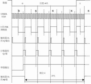
The FSK modulation method of RFID working at 125KHz is very similar. Figure 1 shows a waveform diagram of an FSK modulation method. It can be seen from the figure that the data rate at this time is: carrier frequency fc / 40 = 125K / 40 = 3125bps . After FSK modulation, data 0 is a square wave with frequency fc / 8 , ie f0 = fc / 8 ; and data 1 is a square wave with frequency fc / 5 , that is f1 = fc / 5 .
The transmission data after FSK modulation is transmitted to the PCD through the load modulation method . Figure 1 also shows the RF waveform. The modulation of the carrier is amplitude modulation.
FSK demodulation
After PCD carrier demodulation ( usually envelope detection ) , amplification filtering and pulse shaping circuit, FSK modulation signal is obtained . The FSK demodulation circuit completes the restoration of the FSK modulated signal to the NRZ code. There are many ways to realize FSK demodulation. An FSK demodulation circuit introduced in this paper is shown in Figure 2. This circuit is simple and convenient, and can complete FSK demodulation well.
The working principle of the circuit shown in Figure 2 is as follows: trigger D1 turns the input FSK signal into a narrow pulse, that is, when Q is high, the FSK upper edge sets Q terminal high, but because Q is low at this time , CL terminal is low , And the Q terminal returns to low level. This pulse at the Q terminal resets the decimal counter 4017 to zero and recounts .
The 4017 counter counts the 125KHz clock . Since the data width is 40 / fc = 40Tc (Tc is the carrier period ) , if it is data 0 , the FSK square wave period T0 = ​​8Tc . When the 7th clock is counted, the Q7 output is high, so that CLken (CLK enable terminal ) is high, the counter no longer counts the 8th clock, at this time Q7 is high, when the Q output of the flip-flop D1 is down When a FSK waveform jumps up, the Q terminal output of flip-flop D2 is low. The FSK waveform jumps up and resets the counter to zero again. Thus, the FSK data corresponding to the frequency of the waveform of 0, Q output of the flip-flop D2 is low, that is, data 0 of the NRZ code level.
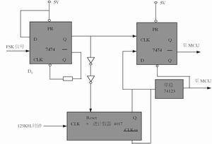
Picture 2 Â FSK demodulation circuit
Picture 3 Â Legend of demodulated waveform with digit 0 ( followed by bit 1)
When the data 1, since the FSK waveform period T1 = 5Tc, so the pin Q7 of counter 4017 is always low, during which the Q output of the flip-flop D2 is kept high, that is, NRZ data level one.
The demodulated waveform of data 0 is shown in Figure 3 . Seen from the figure, if the bit 0 is followed 0, then the bit width of 40Tc, followed if the bit is 1, the bit width which is 37Tc, short three clock cycles. Bit 1 is followed bit 1, bit width which remains 40Tc, if it follows bit is 0, then the bit width of 43Tc. Therefore, the interleaving of bit values 0 and 1 does not cause the propagation of bit width errors, but is compensated. ± 3 clock errors will not affect the accuracy of MCU alignment judgment.
Hop monostable circuit produces a change in the CL terminals of the level provided for the normal operation of the flip-flop D2, and also notifies the data output flip-flop D2 is valid MCU thereafter. The monostable circuit can use 74HC123 , which is a repeatable monostable circuit that can automatically start and shut down the demodulator.
RFID chip FSK usually have multiple modes, such as in one of four modes e5551 (Table 1), the analysis of the circuit described above corresponds FSK1a, but FSK1, just to the output terminal Q of the flip-flop D2 That's it. If FSK2 is used , the output of the counter can be changed to Q9 .
For different data rates, only the bit width is different, which does not affect the demodulation result.
Conclusion
This circuit is simple and reliable and has been used in water meter reading heads.
Piezo Transducer,Piezo Audio Transducer,Piezoceramic Transducer,Piezo Pressure Transducer
NINGBO SANCO ELECTRONICS CO., LTD. , https://www.sancobuzzer.com