Circuit function and advantage
The circuit in Figure 1 uses a 16-bit, 6 MSPS successive approximation (SAR) analog-to-digital converter (ADC) and a differential-to-differential driver combination for low noise at low power (signal-to-noise ratio [SNR] = 88.6 dB) Optimized with low distortion (total harmonic distortion [THD] = −110 dBc). This circuit is ideal for high-performance multiplexed data acquisition systems, such as portable digital X-ray systems and security scanners, because the SAR architecture does not suffer from the delays or pipeline delays typically associated with pipelined ADCs when sampling. 6 MSPS sampling rate enables fast sampling of multiple channels with true 16-bit DC linearity performance and serial low-voltage differential signaling (LVDS) interface for low pin count and low digital noise.
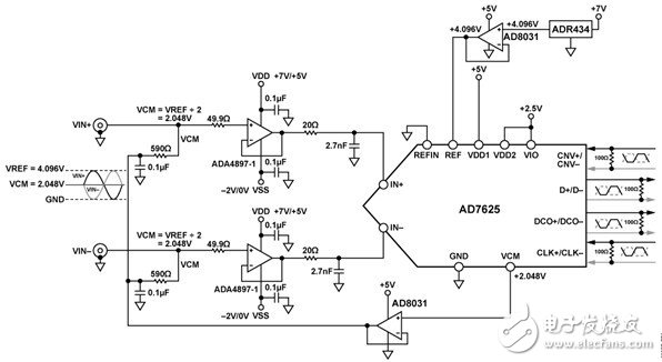
Figure 1. Driving the ADA4897-1 (all connections and decoupling not shown)
The driver uses two low noise (1 nV/√Hz) ADA4897-1 op amps to maintain the dynamic performance of the AD7625 ADC at low power levels (3 mA per amplifier). With a 0.1% fast settling time of 45ns, the ADA4897-1 is ideal for multiplexed applications.
This combination delivers industry-leading dynamic performance at low power in a small board space, the AD7625 is available in a 5 mm &TImes; 5 mm, 32-lead LFCSP package; the ADA4897-1 is available in an 8-lead SOIC package; AD8031 Available in a 5-lead SOT-23 package.
Circuit description
The ADA4897-1 features low distortion (spray-free dynamic range [SFDR] of −93 dB at 1 MHz), 0.1% fast settling time (36 ns), and high bandwidth (230 MHz, −3 dB, G = 1) . The gain of both ADA4897-1 drivers is configured to one. The single-pole 2.95 MHz low-pass RC filter uses a 20Ω resistor and a 2.7 nF capacitor placed between each driver and the ADC. This filter limits the output noise of the op amp at the input of the AD7625 and provides some out-of-band harmonic attenuation.
The common-mode voltage at the ADA4897-1 output is set by buffering the VCM output voltage of the AD7625 (nominally 2.048 V) using the AD8031 configured as a unity-gain buffer. The common mode bias voltage is applied to the input through a 590Ω series resistor. The AD8031 is ideal for driving common-mode voltages because of its low output impedance and fast set-up in the presence of transient currents.
The AD7625 uses the LVDS interface to deliver breakthrough dynamic performance with a signal-to-noise ratio of 92 dB (6 MSPS) and 16-bit (1 LSB) integral nonlinearity (INL) performance. The ADR434 reference (4.096 V) is a low noise, high precision XFET reference with low temperature drift. Its source current output is up to 30 mA and its maximum current sink capability is 20 mA.
The ADR434 is available in an 8-lead MSOP or an 8-lead narrow SOICC package. The AD8031 op amp isolates the ADR434 output from the reference input of the AD7625, providing low impedance and fast settling of the transient current at the REF input.
The dual driver requires only 54 mW, plus 135 mW of ADC power, 12 mW of reference and buffer, and the entire circuit produces only 201 mW of total power.
The circuit uses a +7 V and −2 V supply for the input of the ADA4897-1 driver to minimize power consumption for optimal system distortion performance. The ADA4897-1 output stage is rail-to-rail and swings between 150 mV and 4.85 V when powered from a single 5 V supply. However, an extra 2 V margin at both ends of the range provides low distortion.
Figure 2 shows the circuit AC performance of the input stage using the +7 V and −2 V supplies. SNR = 88.6 dB, THD = −110.7 dB, 20 kHz input signal is 0.6 dB lower than full scale (93% full scale).
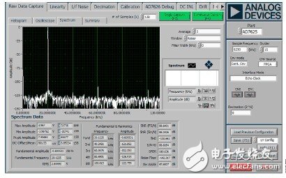
Figure 2. AD7625 and ADA4897-1 powered by dual supply (+7 V, −2 V) with SNR = 88.6 dB, THD = −110.7 dB, fundamental amplitude = −0.6 dB of full scale
Figure 3. AD7625 and ADA4897-1 powered by a single supply (5 V) with SNR = 86.7 dB, THD = -101.1 dB, fundamental amplitude = −1.55 dB of full scale
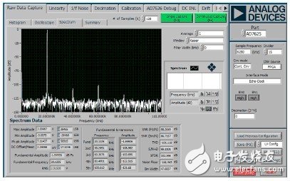
Figure 3 shows the circuit AC performance of the input stage using a single 5 V supply. SNR = 86.7dB, THD = -101.1 dB, and the 20 kHz input signal is 1.55 dB below ground level (84% full scale).
The supply voltage is reduced from −2 V, +7 V to 0 V, + 5V, and the data shows a SNR reduction of approximately 1.9 dB and a THD reduction of approximately 9.6 dB.
The single-supply configuration is suitable for users who do not have dual power supplies but still need high performance.
Common changes
The AD7625 integrates an internal reference and supports two external references if required by the system. The reference voltage is generated by applying the ADR3412 reference (1.2 V) output to the REFIN pin, which is amplified to the correct ADC reference value of 4.096 V through the on-chip reference buffer. The ADR3412 can be powered from the same 5 V analog rail as the AD7625 and features an on-chip reference buffer.
In addition, a 4.096 V external reference (such as the ADR434 or ADR444) can be connected to an ADC unbuffered REF input using a buffer amplifier such as the AD8031, as shown in Figure 1. This method is commonly used in multi-channel applications where the system reference is shared by multiple ADCs.
The ADR434 and ADR444 configurations are also well suited for single-channel applications that require a lower reference temperature coefficient (up to 3 ppm/°C for the ADR434B and ADR444B). The 7 V rail for powering the ADA4897-1 op amp can also power the VIN supply pin of the ADR434 or ADR444.
Another attractive 4.096 V reference is. The ADR4540 low dropout ("300 mV) high precision reference allows operation from a 5 V supply.
If required, the ADA4897-1 and AD8031 single op amps can be replaced with their dual version (ADA4897-2 and AD8032, respectively).
For high input frequencies of 3 MHz, we recommend the ADA4899-1 (15mA/amp) as the driver amplifier.
The ADA4938-1 (37 mA/amp) is ideal for signals up to 10 MHz and can also be used as a single-ended to differential converter.
The performance of this circuit or any high speed circuit is highly dependent on the appropriate printed circuit board (PCB) layout, including but not limited to power supply bypass, controlled impedance lines (if needed), component layout, signal routing, and power and ground planes. .
Capacitor for power transmission and transformation
Capacitor For Power Transmission And Transformation
New Parallel Capacitor 100Kvar,Capacitor Banks,High Voltage Capacitor Banks,Parallel Capacitor 200kar
YANGZHOU POSITIONING TECH CO., LTD , https://www.yzpstcc.com