Scientists at the University of California, Berkeley (UC Berkeley) have said that they have found a new method that can advance the development of on-chip inductor technology and will help create a new generation of micro RF electronic and wireless communications. system design.
Researchers at the University of California are exploring in depth the latest developments in the synthesis of nanomaterials in nanomagnets. According to Liwei Lin, a professor of mechanical engineering at the University of California, Berkeley, researchers have discovered that the use of magnetic nanoparticles with an overlying insulating layer can reduce the size of high-frequency chip inductors while improving performance and, at the same time, increasing The cutoff frequency provides good magnetic permeability, which reduces eddy current losses during high frequency operation.
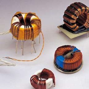
Chip Inductors: The problem often faced by messenger engineers who subvert traditional circuit designs is that while trying to reduce the size of chip inductors, they must maintain their optimal inductance and performance. Liwei Lin said that these difficulties mainly come from the restrictions caused by "basic science and engineering practice constraints."
Chip inductor technology does not evolve as much as transistor technology. Transistor technology has followed Moore's Law for the past 40 years. Inductors are considered to be a passive component on the circuit and are classified in the field of "surpassing Moore's Law." Therefore, non-digitalized functions such as RF and MEMS that do not shrink due to Moore's Law are integrated.
The chip inductor architecture requires a larger area because of the length, number of turns, thickness, and space required between its metal traces to achieve proper inductance and performance. However, for a larger area, inductance loss may occur due to a parasitic effect between the rotating coil and the semiconductor substrate.
Therefore, inductors must be added with magnetic material when they are miniaturized, but in this respect, they also bring other technical limitations, such as process solutions, compatibility with standard processes, and material stability. LiweiLin said that magnetic materials are in terms of magnetic permeability. There are some restrictions on frequency response.
The new inductor manufacturing technology uses insulated nanocomposite magnetic materials as fillers to reduce chip inductor size and increase inductance by up to 80%, thereby reducing chip inductors by at least 50%. In addition, Liwei Lin emphasized that it also has the potential to extend the operating frequency range from GHz to 10 GHz.
He expects that these advances in inductor technology are expected to be implemented in the chip process in the next 3-5 years.
The Industrial Gigabit Media Converter supports 60-watt PoE budget to drive up to 4 IEEE 802.3af compliant powered devices simultaneously. The PoE feature enables the industrial Gigabit Media Converter an efficient and cost-effective solution for SMB, SOHO and other similar fields to deploy the PoE network for the wireless access points, IP-based surveillance cameras or IP phones anywhere easily and efficiently. To satisfy the increasing demand of PoE for Gigabit Ethernet (GE) networking, N-net has developed this series of PoE GE switch.industrial gigabit Media Converter which provides10/100/1000M 802.3af PoE copper ports and 1000Base-X fiber ports.
Industrial Gigabit POE Media Converter
Industrial Gigabit POE Media Converter,Industrial Gigabit Media Converter,POE Media Converter,Industrial Gigabit Fiber Converter,Hardend Gigabit POE Media Converter, Industrial 10/100/1000M POE Media Converter
Shenzhen N-net High-Tech Co.,Ltd , http://www.nnetswitch.com