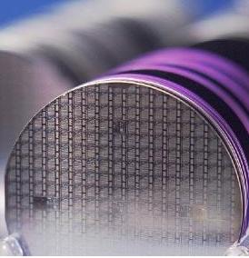
As the basic material of microelectronics and optoelectronics technology, its development has attracted much attention. In particular, today's semiconductor technology has progressed from micron to nanoscale. The more appropriate title for microelectronics is "nanoelectronics," and there will also be an updated demand for semiconductor material properties.
The scale of the Chinese mainland market will further increase the share of 248nm photoresist materials needed in the Chinese mainland market in the global market since 2013.
According to the data released by the China Semiconductor Association in November 2013, the domestic market for semiconductors in mainland China grew from US$74 billion in 2008 to US$112.4 billion in 2012. China is already the world's largest semiconductor consumption area. It is estimated that by 2016, the domestic semiconductor market in Mainland China will further increase to 160 billion US dollars. Raising the self-production rate of semiconductor products has become the policy direction of the semiconductor industry in mainland China.
However, in terms of foundry industry, in addition to SMIC, Huali Microelectronics and Wuhan Xinxin, wafer foundry owners mainly use 8-inch wafer fabs and even 6-inch wafer fabs. The scale of production capacity, process technology and other aspects can not directly compete with international giants such as TSMC and GolbalFoundries. Therefore, some time in the future, foundries in mainland China will seek to grow through three major strategies: “process upgradeâ€, “expanding capacityâ€, and “platform differentiation†in order to effectively increase market share and broaden the living space. In this case, Driven by strong market demand, China's share of the global photoresist material market will surely increase significantly. According to the above table, the market share of G-Line photoresist materials required in the Chinese mainland market has increased significantly since 2012; the share of I-Line photoresist materials required in the global market has increased significantly since 2013 The required share of 248nm photoresist in the global market has increased significantly since 2013.
Yongguang Chemical has been operating the Chinese mainland market for many years and has established a smooth and flexible distribution and supply network. In addition to establishing a production base in Suzhou, Everlight Chemicals can more easily understand customer needs and penetrate the market. In 2011, it also acquired East China distributor Aetna Semiconductor (Suzhou) Co., Ltd. to become a subsidiary of Everlight Group, which can further strengthen its relationship with China. Continental customer service. Let customers really feel the local production, tailored, real-time service, price-quality services.
Dedicated to the development of high-resolution materials In order to meet the temperature conditions during the ion implantation process, material manufacturers will develop more heat-resistant photoresists.
The continuous emergence of new technologies in the semiconductor industry also promotes the continuous evolution of materials technology. The semiconductor process is progressing toward a thinner line width, and the development of an I-Line high-resolution photoresist (EPI626, film thickness of 1 μm, resolution of 0.35 μm) continues to be a trend in the market. In addition, in order to meet the temperature conditions during the ion implantation process, material manufacturers will develop more heat-resistant photoresists to increase product competitiveness. However, currently, the foundry industry in China still uses 8-inch wafers as the main production capacity, and the 0.18-micron/0.15-micron/0.13-micron process is the mainstream process. Everlight will continue to focus on the research and development of thin lines and high resolution, and strive to develop DUV photoresist.
In terms of IC packaging applications, smart phones and other products emphasize thinness and drive the development of high-density packaging technologies, including high-end packaging technologies such as wafer-level packaging (WCSP), through-silicon vias (TSV), and micro bumps. Material manufacturers should actively develop photoresists and bumps thick film photoresists for silicon perforation processes (positive type: EPG590Series, film thickness 10-30μm, resolution <10μm; negative type: ENPI503, film thickness 20μm, Resolution <8μm) to meet market demand.
In the application of LED process, the LiftOff process can eliminate the strong acid precious metal process, in line with the trend of environmental protection, has gradually become an important direction in the industry, improve the heat resistance of the photoresist to increase its process tolerance is a development direction. In addition, the lighting market is already the mainstream of LED applications. Patterned PSS on the surface of sapphire wafers can significantly increase LED luminous efficiency. Therefore, it is necessary to continuously develop high-resolution PSS photoresists. In the polishing and polishing process of the sapphire substrate upstream of the LED, since the C-plane sapphire substrate is widely used in the LED epitaxial process, the A-plane sapphire substrate is also used in the protective film of the optical lens and the 3C product, and it is foreseen that the LED sapphire grinding will be performed in the next few years. The market for polishing liquids will thrive. Therefore, in the future, we will develop polishing fluid-related products for 2†to 6†sapphire wafers.
Yongguang Chemical established the Electronic Chemistry Division in 1998. After more than ten years of research and development and technological advancement, I-line key layer photoresist EPI626 was successfully launched with a resolution of less than 0.35 μm, plus the best resolution G-in the market. The line photoresist EPG535 forms a complete product layout on the semiconductor process G/I-Line photoresist.
Everlight will continue to develop more advanced and higher quality photoresists in the I-Line yellow lithography process. The marketed EPI626 is I-Line's higher resolution key layer photoresist (8-inch wafer fab) . Its yellow lithography process has a resolution of 0.35μm; good heat resistance, good adhesion, high photosensitivity (lower exposure energy), greater process tolerance, easier processing on the process, and better resolution Other characteristics.
For thick film photoresists, they are mainly supplied to silicon wafer fabs and passive component manufacturers. They have high penetrability and good adhesion properties. After the yellow light process, the thick film photoresist presents a vertical circular shape. In gold and copper electroplating process, as well as the production of gold bumps or copper lines, under the different parameters of the yellow light process operation, the photoresist pattern can maintain high resolution and no embrittlement.
850nm IR LED(infrared LED) manufacturer from China.
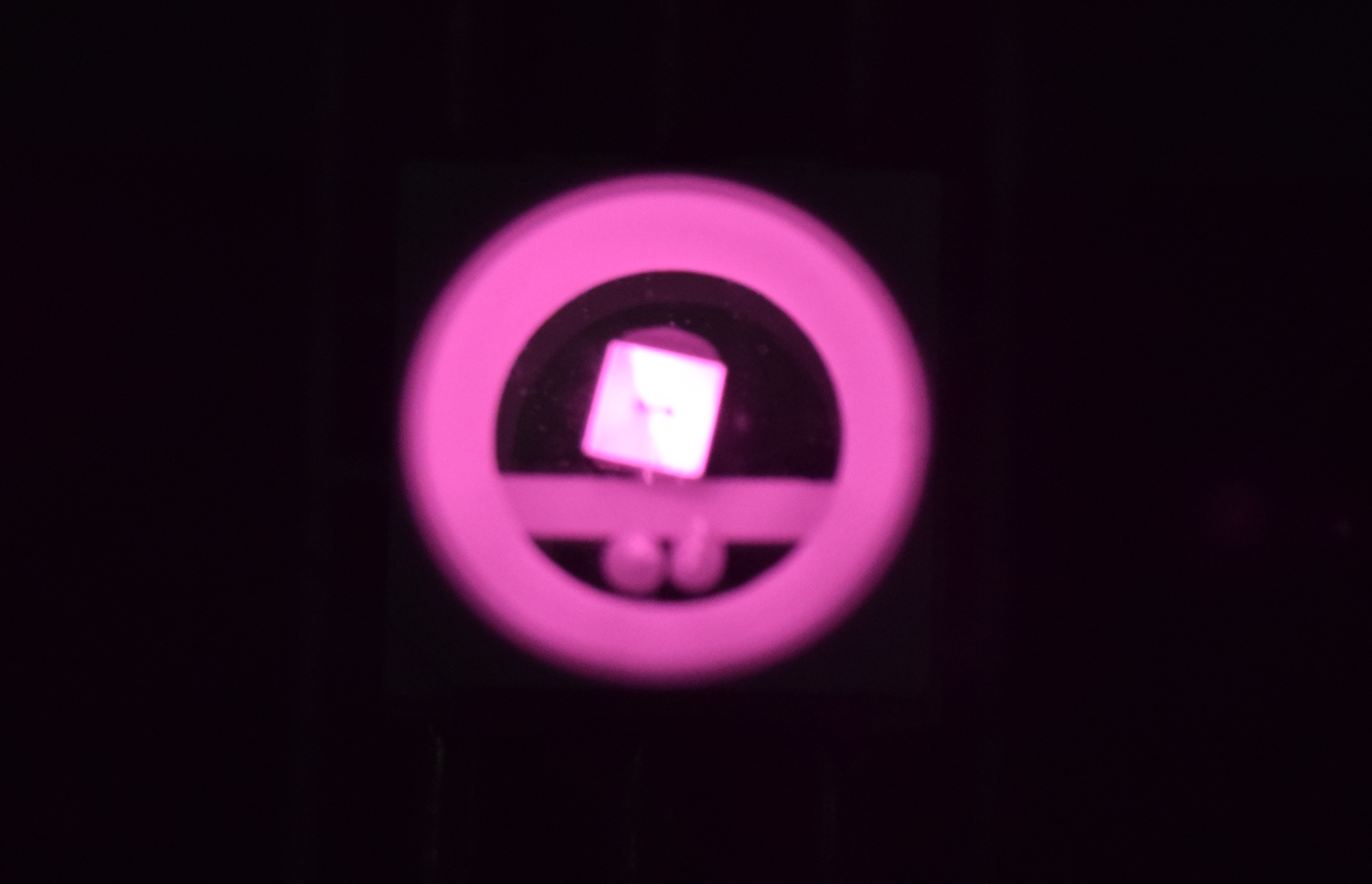
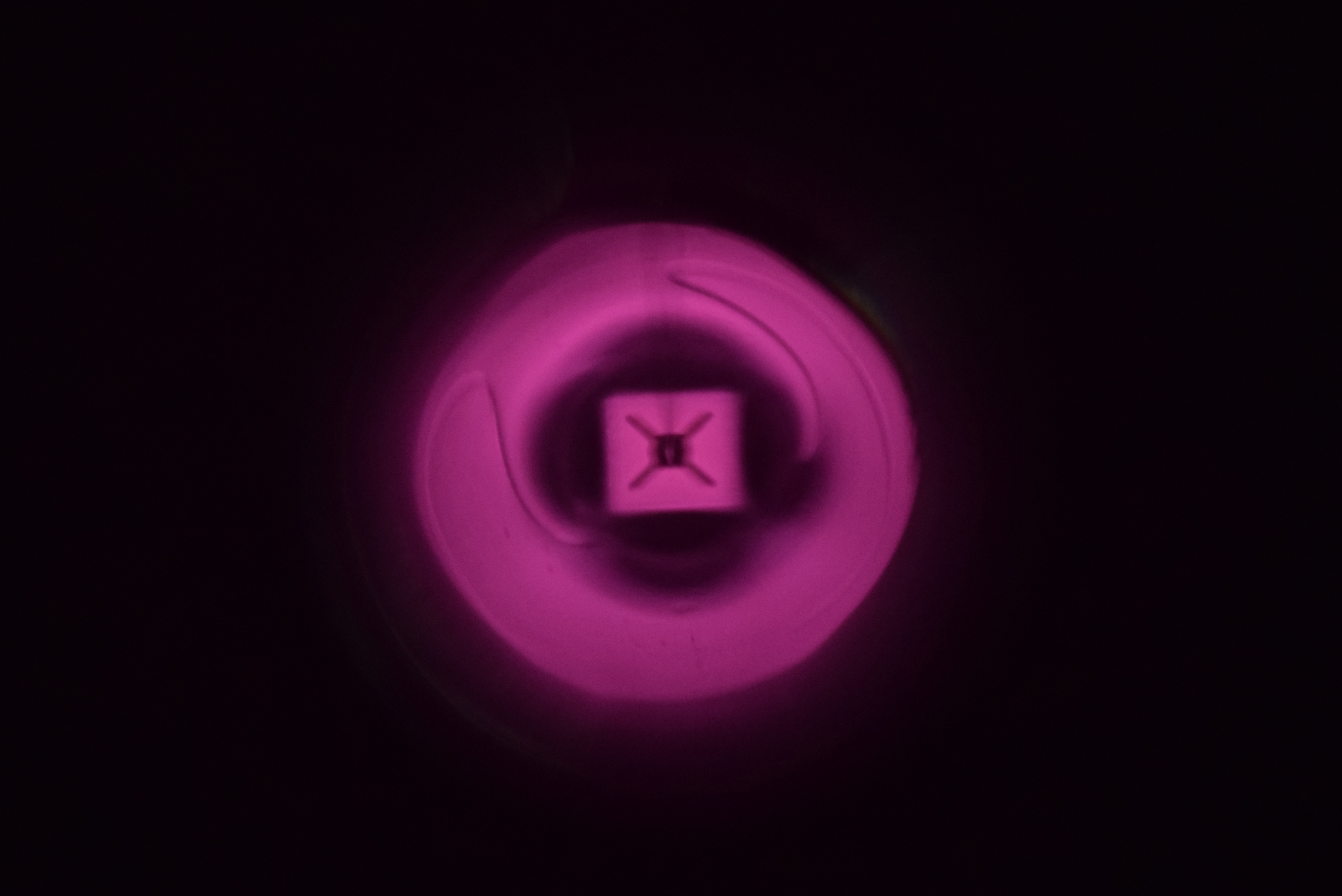
850Nm IR LED, it's different from 940nm IR LED, you can see some weak red bright when the 850nm IR LED is working. Widely used in street monitoring, underground market yard monitoring, infrared sensors, infrared monitoring, infrared touch screen, etc.


Raw materials use the LED chip from Taiwan Epistar, Tyntek, Optotech. The stability of our products have been recognized by all of our custom.

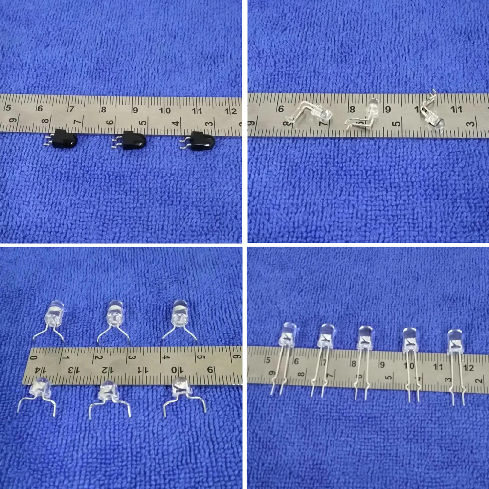
For the lens of LED, 850nm Through-hole IR LED with wanter clear lens, black lens, navy blue lens are available.
The angle of the LED is selectable too, for instance: 5 degree 850nm Through-hole IR LED, 20 degree 850nm Through-hole IR LED, 30 degree 850nm Through-hole IR LED, 45 degree 850nm Through-hole IR LED, 60 degree 850nm Through-hole IR LED, 90 degree 850nm Through-hole IR LED, 120 degree 850nm Through-hole IR LED ect.
Shape can be: Straw hat, oval, flat top and short head 850nm Through-hole IR LED ect.
Size can be: 5mm round 850nm Through-hole IR LED, 3mm round 850nm Through-hole IR LED, 5mm straw hat 850nm Through-hole IR LED, 3mm flat top 850nm Through-hole IR LED,5mm flat top 850nm Through-hole IR LED, 8mm round 850nm Through-hole IR LED, 8mm straw hat 850nm Through-hole IR LED, 3*4*6mm 850nm Through-hole IR LED, 5*4*6mm oval 850nm Through-hole IR LED, 2*3*4mm square 850nm Through-hole IR LED, 4mm falt top 850nmThrough-hole IR LED and so on.
All of our product are meet with Reach, CE, RoSH, SGS, EN62471 standards and have 5 years warranty.
850nm Through-Hole IR LED
850nm Through-Hole IR LED,Through-hole LED IR 850nm,IR 850nm 3mm Through-hole LED
Shenzhen Best LED Opto-electronic Co.,Ltd , https://www.bestsmd.com