More detailed image
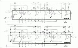
Figure 1. Configured as shown, two filter ICs reconstruct the output of D / A converter while providing antialiasing and sinc-compensation functions.
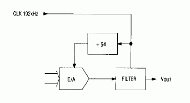
Figure 2. In a suggested application for the Figure 1 circuit, the applied clock signal and single-chip divider set the desired sample rate for the D / A converter.
At, DC, a D / A converter's output is easily predicted from it's datasheet specs. Time-varying signals, however, produce staircase-output waveforms whose reconstruction errors are best discussed in the frequency domain. The converter's output spectrum, for example, consists of spectra (± f1, where f1 is the spectrum represented by the digital input samples) that repeat at integral multiples of the sample rate fS (Figure 3).
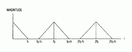
Figure 3. Figure 2's digital-input spectrum F1 combines with the D / A converter's sampling rate fS as shown, producing a ± f1 spectrum that repeats at integral multiples of fS.
The filter's first job is to prevent alias frequencies by excluding spectral energy above fS / 2. In practice, f1 <fS / 2. The filter should pass f1 with an acceptably low error while sufficiently attenuating all frequencies above fS / 2.
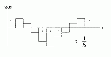
Figure 4. Before filtering, the D / A converter's output signal is a staircase waveform that can be regarded as a sequense of rectangular pulses.
A second filter requirement stems from the presence of sinc attenuation, introduced by the effect of rectangular-pulse components in the staircase waveform (Figure 4). These pulses have the same 1 / fS width, but differ in amplitude according to the digital-sample magnitudes. The spectrum of each pulse is the Fourier transform (the sinc function of f / fS). These spectra combine with the f1 spectrum to form an overall frequency response for the converter output. Note the sinc expression's variation in amplitude for various values ​​of f:
Table 1.
| f | [(sin) (Ï€f / fS] / (Ï€f / fS) |
| 0 | 1.0 |
| fS / 4 | 0.9003 (-0.9dB) |
| fS / 3 | 0.8270 (-1.65dB) |
| fS / 2 | 0.6366 (-3.92dB) |
Clearly, the staircase approximation causes an increase amplitude error as f approaches the Nyquist frequency fS / 2. To compensate for this attenuation, the Figure 1 circuit incorporates the inverse expression (Ï€f / fS) / sin (Ï€f / fS) in it's passband- magnitude response.
Ideally, the resulting filter response would provide sinc compensation to fS / 2, drop abruptly to zero, and maintain that infinite attenuation for all frequencies above fS / 2. But actual filters cannot provide abrupt transitions or infinite attenuation. As a practical compromise, the circuit makes its transition over a finite bandwidth (transition ratio), and then provides an out-of-band rejection comparable to the D / A converter's signal-to-noise ratio SNR.
SNR for an ideal D / A converter is about 6dB / bit, or 72dB for a 12-bit device. Quantization error further degrades this number, yielding about 68dB for a typical 12-bit converter. Thus a reasonable goal in Figure 1 is 70dB rejection above fS / 2.
To prevent aliasing, the stopband edge must be no greater than the Nyquist frequency (fS / 2). The passband edge must threrfore be less than fS / 2. To achieve 70dB stopband rejection in the 8th-order circuit of Figure 1, the required transition ratio (fStopband / fPassband)) is 1.5, which sets the passband edge at fS / 3. A rising amplitude response within this passband compensates for the converter's sinc attenuation.
Perfect sinc compensation would provide 1.65dB of gain at the Nyquist frequency, but tolerance uncertainties in the ± 1% resistors and within the filter ICs limits the actual correction to about 1dB. The circuit does, however, achieve the 70dB stopband rejection and the 1.5 transition ratio. Figure 5 compares the Figure 1 response with that of an ideal filter.
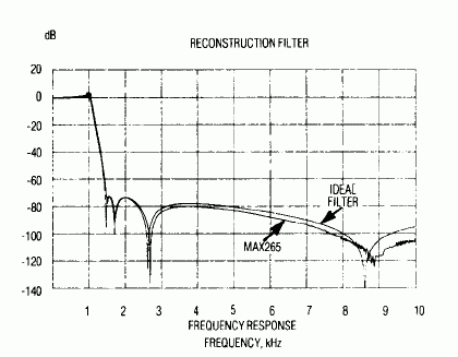
Figure 5. The circuit response of Figure 1 compares well with that of an ideal filter.
To assure maximum dynamic range, the four biquad-filter sections (two in each IC) exhibit increasing Q from input to output, The pole-zero pairs of each section also axhibit increasing frequency, which minimizes the spread in component values. The following pole and zero values ​​produce a 1-rad / sec filter passband:
Table 2.
| Section | fpole (Hz) | Qpole | fZero (Hz) |
| 1 | 0.1005 | 0.5603 | 0.2397 |
| 2 | 0.1310 | 1.0540 | 0.2777 |
| 3 | 0.1564 | 2.3876 | 0.4273 |
| 4 | 0.1685 | 8.5145 | 1.4016 |
Note the feedback capacitors C1-C4 across each output op amp. These capacitors have two purposes; they improve the quality of transmission zeroes, and the form 1-pole lowpass filters that help to smooth out the discrete-level steps introduced by the filter's switched -capacitor action. The 1-pole filters have little effect on the passband shape because their high corner frequencies introduce only 0.1dB of loss at 1kHz.
Note also, that the applied clock frequency in Figure 2 (192kHz) allows use of a convenient binary-64 divider for setting the necessary 3X ratio betweeen the converter's sample rate and the filter's 1kHz corner frequency, f0. Each chip is programmed for an fCLK / f0 ratio of 191.64 by V + and V- connections to the filter inputs, F0-F5.
MOSO Class II Programmable LED Driver supports 0-10V, PWM, timer step dimming or DALI control from 75W to 320W. It can reprogram the output by a software or infrared controller. Class II outdoor Driver is IP67 waterproof, with build-in surge protection. It provides a Dim-to-off mode with low standby power. MOSO Class II Programmable power uses extruded-metal housing and fully glue-potted for good dissipation.


MOSO developed Class II Programmable LED Driver series with special isolation design for global market especially for the Europe. All Class II LED Drivers are certified with CCC, CE, TUV, ENEC and CB standards.
MOSO has set several distributors in Europe, United States, Latin America, Asia and Australia. All MOSO Class II Programmable power suppliers provide 5 years global warranty. In case of any failure, customers can get replacement either from MOSO directly or any one of MOSO distributors.
MOSO always dedicates to providing professional outdoor lighting solutions. Please feel free to contact our sales team if you need any support!
Class II Programmable LED Driver
Class II Programmable LED Driver,Class II Programmable Dimmable Driver,Dim-to-off Class II Programmable Driver,Class II Programmable Outdoor LED Driver
Moso Electronics , https://www.mosoleddriver.com