Abstract: This arTIcle provides an understanding of the effects of digital crosstalk coupling onto analog signal lines. Typical mechanisms of digital crosstalk include power supply coupling, capaciTIve crosstalk, and grounding currents.
What is the effect of digital signal bits cross-talking into the analog secTIon of a data-conversion system? There is a lot written into the data sheets of ADCs and DACs on how to minimize it. But, when asked what is the result, most laymen have the insight that "it creates noise". While this is a very true statement, there is value to understanding this at a deeper level, so that a design engineer can more efficiently understand and troubleshoot a broken circuit. After reading this arTIcle , the reader will understand that harmonic distortion and other signal-dependant-error problems can be caused by crosstalk from digital signal bits, which can take a long time to fix if the mechanisms are not understood. Sources of CrosstalkOur system, for analysis purposes, consists of a pure sine wave signal generator, feeding an ADC, with a clean sample clock. The ADC sends its data to a memory or other CPU for FFT processing. This analysis also applies to a DAC system, in which digital data is ge nerated from a memory or other CPU, and is sent to a DAC, and measured with a spectrum analyzer. The degradation due to this crosstalk is more pronounced and easier to understand in parallel data converter systems, although the analysis also applies to serial data converter systems.
The typical mechanisms of cross talk include: Power supply coupling: digital currents pulling on a power supply that is shared with an analog supply, which causes the supply to move with the bit, which gets into the signal path through an amplifier's supply pin (when the amplifier does not have an infinite power supply rejection ratio). This problem gets eliminated by (in order of effectiveness) using different power supplies for the analog and digital circuitry, or putting a low pass filter between the analog and digital circuitry, or by better capacitive bypassing.
Capactive crosstalk: when digital signals are run near analog signals, the capacitance between the lines can cause the lines to couple and move together. This problem gets eliminated by running the analog signals in a separate routing area than the digital, and by putting grounding shields between the analog and the digital.
Grounding currents: the digital return currents return ground through a non-zero impedance, due to either resistive or inductive effects, which can cause the local "ground" to move up and down with the currrent. If this ground differs from the originator of the signal, this will cause voltage differences at the rate of the bits. This problem gets eliminated by improving grounding, or by understanding and controlling the paths that ground current flows in. Using differential signals, both analog and digital, can reduce the effect of all of the above problems. To the effect that the analog signal is differential and the crosstalk has equal coupling on both sides of the differential signal (in both amplitude and phase), and the analog receiver has a good common mode rejection ratio, the crosstalk will not be seen differentially. To the effect that the digital bits are differential and balanced (both rise / fall timing, and amplitude) the positive signal will have an equal and opposite effec t as the negative polarity signal. Hence, the offending crosstalk from net coupling effects, capacitive crosstalk, and grounding effects is cancelled. Note: differential systems can only be realized to finite perfection, so designing with differential analog signals and digital signals only create first order fixes to the problem in real systems; best performance demands use of all best practices. Analysis and Implications of Crosstalk In analyzing the crosstalk effects, the key concept to understand is that the frequency domain content of digital signal bits is not "random noise". Any digital signal bits are a strictly deterministic function of the analog signal they represent. Each bit of the conversion process is a non-linear, non-monotonic function of the analog signal. Hence, the error caused by the digital cross talk is a signal -dependant error. Also hence, as in any non-linear memory-less system, all of the energy in the digital signal bits is exclusively in the harmonics of the signal they represent (this will be illustrated below). The exception comes from the fact this is a sampled system, the higher harmonics that exceed the nyquist rate will alias back into the nyquist band at the predictable frequency locations. An additional exception is the noise in the original signal itself, which we are assuming in this analysis to be small. There is no energy in this system at any other frequency. Hence, these effects can be very predictable, and far from random (sometimes the relationship can become complicated such that it seems random, but it is not random).
A key implication to the above is that often a digital bit crosstalk problem is manifested as a harmonic distortion or signal dependant error problems. Harmonic distortion problems are typically troubleshot by investigating the linearity of the amplifiers that drive an ADC, or by suspecting whether the ADC is living up to its specified linearity performance. Signal dependant error problems often get an additional suspicion of frequency domain flatness in the analog signal chain or data converters. With this new understanding, any harmonic distortion or signal-dependant-error troubleshooting effort should always include suspicion of digital crosstalk, and the mechanisms listed above.
To gain more intuition as to why digital bits only contain the harmonics of the signal they represent, we merely need to look at the bits closely. The easiest to understand is to look at the MSB of an ADC sampling a DC-centered sine wave ( see Figure 1). The MSB is merely a square wave at the same frequency as the sine wave. This same frequency relationship is true independent of the selection of the input frequency and sampling frequencies; any deviation shows up as a deterministic jitter on the square wave edges, which can be analyzed through sampling theory, which will not be elaborated upon in this article.
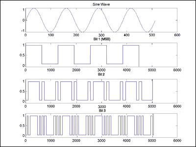
Figure 1. Sine wave, and top three resulting MSB's.
This square wave bit can now be looked at for its frequency domain components. A square wave has as its frequency components, the fundamental, and its odd harmonics (see Figure 2). This example shows a square wave at a frequency of 8 cycles per total samples captured. (this is FFT-bin-frequency 8), which has energy at frequencies of 1 × 8 = 8, 3 × 8 = 24, and 5 × 8 = 40. Even harmonics would be present if the sine wave was not DC-balanced, which will be illustrated below.
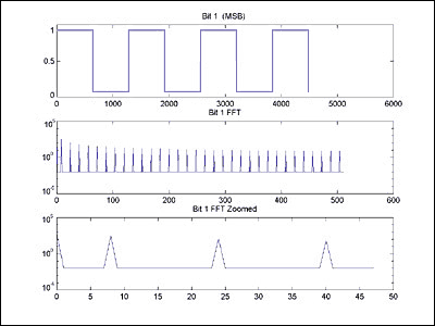
Figure 2. Sine wave MSB, its FFT, and a zoomed-in view of the FFT.
The rest of the bits also have their energy exclusively at the harmonic frequencies of the signal the bits represent (See Figure 3 and 4). To get intuition behind this refer back to Figure 2, and notice that the lower order bits have a pattern that repeats with the same period as the input signal. Another observation to make from Figures 3 and 4 is that the lower the order of the bits, the more the energy gets distributed into the higher harmonics.
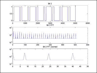
Figure 3. Sine wave 2nd MSB, its FFT, and a zoomed-in view of the FFT.
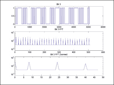
Figure 4. Sine wave 2nd MSB, its FFT, and a zoomed-in view of the FFT.
Converging towards the bottom line, if these bits coupled into the analog signal, they would add the frequency content that was just viewed. To simulate a net effect of this, a sine wave was simulated, and the three highest order bits were added in at a 1%, 40dB level each. Figure 5 shows a zoomed in FFT plot of the original signal, and the corrupted signal. What is your first reaction to reduce this distortion?
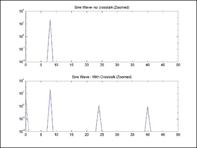
Figure 5. Zoomed-in FFT plot of a pure sine wave, and the same sine wave corrupted by 1% coupling from the three highest order digital signal bits.
As alluded to above, if the analog signal is not balanced across the zero crossing (ie has DC offset), the digital bits will not be balanced / symmetric, and hence the even harmonics are also created (Figure 6, 7, and 8) .
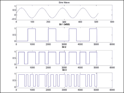
Figure 6. DC-unbalanced (offset) sine wave, and top 3 resulting MSB's.
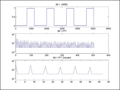
Figure 7. DC-unbalanced (offset) sine wave, and top 3 resulting MSB's.
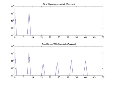
Figure 8. Zoomed-in FFT plot of a pure DC-unbalanced (offset) sine wave, and the same sine wave corrupted by 1% coupling from the three highest order digital signal bits.
The above example was carefully chosen to illustrate the point. FFT-bin-Frequency 8 (for a system whose sample set is comprised of a power of 2) forces all aliased harmonics to fall on top of the in-band harmonics. Another way of describing the relationship is that there are many common factors (in this case, all) between the number of cycles of the original sine wave in the sample set, and the number of samples. To the effect that this relationship is reduced, the aliased harmonics will show up at other predictable frequencies. Figure 9 shows the net result to Figure 8 if the input frequency is moved to FFT-bin-Frequency 6, which allows the upper harmonics to fall in other locations than on top of the harmonics. Again, Since the signal is balanced, only odd harmonics are generated. The figure shows the strongest interfering energy is still at the odd harmonics at 6, 18, and 30. However, observe in the figure that energy exists at frequencies 2, 14, and 26 , which correspond with aliase s from harmonics 171, 173, and 175 respectively. Energy is also at 10, 22, and 34, which corresponds with harmonics 169, 168, and 167 respectively. The most general statement is that a harmonic can alias into any frequency that has a common multiple between the input signal and the sample rate.
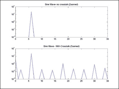
Figure 9. Zoomed-in FFT plot of a pure DC-balanced sine wave at FFT-Frequency-Bin 6, and the same sne wave corrupted by 1% coupling from the three highest order digital signal bits. ConclusionDigital signal cross talk can be mysterious and chaotic. However, it can cause problems, such as harmonic distortion and signal dependant errors that can be difficult to troubleshoot if it is not understood that the mechanism is the crosstalk. Armed with this knowledge, a designer can become a better troubleshooter and ultimately design a high performing system.
What is the effect of digital signal bits cross-talking into the analog secTIon of a data-conversion system? There is a lot written into the data sheets of ADCs and DACs on how to minimize it. But, when asked what is the result, most laymen have the insight that "it creates noise". While this is a very true statement, there is value to understanding this at a deeper level, so that a design engineer can more efficiently understand and troubleshoot a broken circuit. After reading this arTIcle , the reader will understand that harmonic distortion and other signal-dependant-error problems can be caused by crosstalk from digital signal bits, which can take a long time to fix if the mechanisms are not understood. Sources of CrosstalkOur system, for analysis purposes, consists of a pure sine wave signal generator, feeding an ADC, with a clean sample clock. The ADC sends its data to a memory or other CPU for FFT processing. This analysis also applies to a DAC system, in which digital data is ge nerated from a memory or other CPU, and is sent to a DAC, and measured with a spectrum analyzer. The degradation due to this crosstalk is more pronounced and easier to understand in parallel data converter systems, although the analysis also applies to serial data converter systems.
The typical mechanisms of cross talk include: Power supply coupling: digital currents pulling on a power supply that is shared with an analog supply, which causes the supply to move with the bit, which gets into the signal path through an amplifier's supply pin (when the amplifier does not have an infinite power supply rejection ratio). This problem gets eliminated by (in order of effectiveness) using different power supplies for the analog and digital circuitry, or putting a low pass filter between the analog and digital circuitry, or by better capacitive bypassing.
Capactive crosstalk: when digital signals are run near analog signals, the capacitance between the lines can cause the lines to couple and move together. This problem gets eliminated by running the analog signals in a separate routing area than the digital, and by putting grounding shields between the analog and the digital.
Grounding currents: the digital return currents return ground through a non-zero impedance, due to either resistive or inductive effects, which can cause the local "ground" to move up and down with the currrent. If this ground differs from the originator of the signal, this will cause voltage differences at the rate of the bits. This problem gets eliminated by improving grounding, or by understanding and controlling the paths that ground current flows in. Using differential signals, both analog and digital, can reduce the effect of all of the above problems. To the effect that the analog signal is differential and the crosstalk has equal coupling on both sides of the differential signal (in both amplitude and phase), and the analog receiver has a good common mode rejection ratio, the crosstalk will not be seen differentially. To the effect that the digital bits are differential and balanced (both rise / fall timing, and amplitude) the positive signal will have an equal and opposite effec t as the negative polarity signal. Hence, the offending crosstalk from net coupling effects, capacitive crosstalk, and grounding effects is cancelled. Note: differential systems can only be realized to finite perfection, so designing with differential analog signals and digital signals only create first order fixes to the problem in real systems; best performance demands use of all best practices. Analysis and Implications of Crosstalk In analyzing the crosstalk effects, the key concept to understand is that the frequency domain content of digital signal bits is not "random noise". Any digital signal bits are a strictly deterministic function of the analog signal they represent. Each bit of the conversion process is a non-linear, non-monotonic function of the analog signal. Hence, the error caused by the digital cross talk is a signal -dependant error. Also hence, as in any non-linear memory-less system, all of the energy in the digital signal bits is exclusively in the harmonics of the signal they represent (this will be illustrated below). The exception comes from the fact this is a sampled system, the higher harmonics that exceed the nyquist rate will alias back into the nyquist band at the predictable frequency locations. An additional exception is the noise in the original signal itself, which we are assuming in this analysis to be small. There is no energy in this system at any other frequency. Hence, these effects can be very predictable, and far from random (sometimes the relationship can become complicated such that it seems random, but it is not random).
A key implication to the above is that often a digital bit crosstalk problem is manifested as a harmonic distortion or signal dependant error problems. Harmonic distortion problems are typically troubleshot by investigating the linearity of the amplifiers that drive an ADC, or by suspecting whether the ADC is living up to its specified linearity performance. Signal dependant error problems often get an additional suspicion of frequency domain flatness in the analog signal chain or data converters. With this new understanding, any harmonic distortion or signal-dependant-error troubleshooting effort should always include suspicion of digital crosstalk, and the mechanisms listed above.
To gain more intuition as to why digital bits only contain the harmonics of the signal they represent, we merely need to look at the bits closely. The easiest to understand is to look at the MSB of an ADC sampling a DC-centered sine wave ( see Figure 1). The MSB is merely a square wave at the same frequency as the sine wave. This same frequency relationship is true independent of the selection of the input frequency and sampling frequencies; any deviation shows up as a deterministic jitter on the square wave edges, which can be analyzed through sampling theory, which will not be elaborated upon in this article.
Figure 1. Sine wave, and top three resulting MSB's.
This square wave bit can now be looked at for its frequency domain components. A square wave has as its frequency components, the fundamental, and its odd harmonics (see Figure 2). This example shows a square wave at a frequency of 8 cycles per total samples captured. (this is FFT-bin-frequency 8), which has energy at frequencies of 1 × 8 = 8, 3 × 8 = 24, and 5 × 8 = 40. Even harmonics would be present if the sine wave was not DC-balanced, which will be illustrated below.
Figure 2. Sine wave MSB, its FFT, and a zoomed-in view of the FFT.
The rest of the bits also have their energy exclusively at the harmonic frequencies of the signal the bits represent (See Figure 3 and 4). To get intuition behind this refer back to Figure 2, and notice that the lower order bits have a pattern that repeats with the same period as the input signal. Another observation to make from Figures 3 and 4 is that the lower the order of the bits, the more the energy gets distributed into the higher harmonics.
Figure 3. Sine wave 2nd MSB, its FFT, and a zoomed-in view of the FFT.
Figure 4. Sine wave 2nd MSB, its FFT, and a zoomed-in view of the FFT.
Converging towards the bottom line, if these bits coupled into the analog signal, they would add the frequency content that was just viewed. To simulate a net effect of this, a sine wave was simulated, and the three highest order bits were added in at a 1%, 40dB level each. Figure 5 shows a zoomed in FFT plot of the original signal, and the corrupted signal. What is your first reaction to reduce this distortion?
Figure 5. Zoomed-in FFT plot of a pure sine wave, and the same sine wave corrupted by 1% coupling from the three highest order digital signal bits.
As alluded to above, if the analog signal is not balanced across the zero crossing (ie has DC offset), the digital bits will not be balanced / symmetric, and hence the even harmonics are also created (Figure 6, 7, and 8) .
Figure 6. DC-unbalanced (offset) sine wave, and top 3 resulting MSB's.
Figure 7. DC-unbalanced (offset) sine wave, and top 3 resulting MSB's.
Figure 8. Zoomed-in FFT plot of a pure DC-unbalanced (offset) sine wave, and the same sine wave corrupted by 1% coupling from the three highest order digital signal bits.
The above example was carefully chosen to illustrate the point. FFT-bin-Frequency 8 (for a system whose sample set is comprised of a power of 2) forces all aliased harmonics to fall on top of the in-band harmonics. Another way of describing the relationship is that there are many common factors (in this case, all) between the number of cycles of the original sine wave in the sample set, and the number of samples. To the effect that this relationship is reduced, the aliased harmonics will show up at other predictable frequencies. Figure 9 shows the net result to Figure 8 if the input frequency is moved to FFT-bin-Frequency 6, which allows the upper harmonics to fall in other locations than on top of the harmonics. Again, Since the signal is balanced, only odd harmonics are generated. The figure shows the strongest interfering energy is still at the odd harmonics at 6, 18, and 30. However, observe in the figure that energy exists at frequencies 2, 14, and 26 , which correspond with aliase s from harmonics 171, 173, and 175 respectively. Energy is also at 10, 22, and 34, which corresponds with harmonics 169, 168, and 167 respectively. The most general statement is that a harmonic can alias into any frequency that has a common multiple between the input signal and the sample rate.
Figure 9. Zoomed-in FFT plot of a pure DC-balanced sine wave at FFT-Frequency-Bin 6, and the same sne wave corrupted by 1% coupling from the three highest order digital signal bits. ConclusionDigital signal cross talk can be mysterious and chaotic. However, it can cause problems, such as harmonic distortion and signal dependant errors that can be difficult to troubleshoot if it is not understood that the mechanism is the crosstalk. Armed with this knowledge, a designer can become a better troubleshooter and ultimately design a high performing system.
Dog Training Transmitter,Vibration Training Collar,Remote Control Vibration Collar,Rechargeable Dog Shock Collar
Elite-tek Electronics Ltd , https://www.aetertek.ca