The IS-95 and 3GPP spread spectrum wireless communication standards impose strict requirements on the linearity and adjacent channel power ratio (ACPR) of RF power amplifiers. To meet these specifications, high-linearity Class A or Class AB RF power amplifiers are typically used in W-CDMA handsets. However, at an output power of +28 dBm, the power added efficiency (PAE) of such amplifiers rarely exceeds 35%. As the output power decreases, PAE drops even further, which poses a challenge for energy efficiency.
Power amplifiers do not operate continuously during calls. When users are not speaking, the amplifier runs at half rate (50% duty cycle) or even 1/8 rate, reducing heat generation. However, in data mode, the power amplifier remains active until the data transmission is complete. This continuous operation combined with low efficiency can rapidly drain the battery and cause overheating in the device.
Battery life has always been a critical issue for early W-CDMA handsets that support high-speed data services. Designers had to incorporate larger heat sinks, stronger cooling systems, and higher-capacity batteries to manage thermal and power issues. Fortunately, recent improvements in power amplifier efficiency have significantly reduced these challenges.
In CDMA and W-CDMA systems, the RF power output of the power amplifier is not always at its maximum. To optimize cellular capacity—i.e., the number of simultaneous channels a base station can handle—each handset must adjust its RF output power so that the signal-to-noise ratio received by the base station remains consistent.
Based on statistical data from many mobile phones in a given area, the average RF output power of a standard CDMA or W-CDMA phone is about +10 dBm in suburban areas and around +5 dBm in urban environments. Therefore, improving power amplifier efficiency should focus on optimizing performance between +5 dBm and +10 dBm rather than just maximizing output power.
CDMA and W-CDMA power amplifiers require two supply voltages: VREF, which biases the internal driver and power amplifier stages, and VCC, which biases the collector of the driver and power amplifier. By adjusting these voltages, designers can reduce the supply current and improve overall efficiency.
When the RF transmit power is zero, the power amplifier automatically reduces the quiescent current to approximately 100 mA (typical), with VREF at 3V and VCC at 3.4V. Lowering VREF from 3V to 2.9V can reduce the quiescent current by around 20 mA, helping to conserve power.
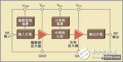
F1: CDMA/W-CDMA power amplifiers require two supply voltages: Vref and Vcc. Adjusting these voltages allows the designer to reduce the operating current of the power amplifier. Lowering VREF can significantly reduce the quiescent current, provided that the power amplifier's linearity and ACPR remain within specification.
Reducing both VREF and VCC can help lower power consumption. If we have empirical data indicating the minimum VREF required for different output power levels, it becomes possible to actively control VREF based on the power amplifier’s output level. Alternatively, a two-stage regulation approach can be used, where VREF is adjusted for low-power (below +10 dBm) and high-power (above +10 dBm) modes.
To adjust VREF using a digital-to-analog converter (DAC), a low-power operational amplifier with high output current capability and external gain adjustment is typically used. In most handsets, VCC is derived directly from a single-cell Li-ion battery, which operates between 3.2V and 4.2V. Statistical data shows that CDMA and W-CDMA power amplifiers mostly operate at +5 to +10 dBm, allowing for significant reductions in VCC without sacrificing linearity.
Experimental tests have shown that as long as the collector bias remains below 0.6V, normal communication with the base station is still possible. A variable bias voltage is applied to the power amplifier’s collector via a high-efficiency DC/DC buck converter. A dedicated DAC output from the baseband processor can control this converter’s output voltage. The DC/DC converter must respond quickly to changes in the control signal, ideally reaching 90% of the new set voltage within 30 microseconds.
The converter die includes internal gain between its VCC control input and the collector bias voltage. It also switches at high frequencies to minimize the size of the inductor. Connecting a DC/DC converter between the power amplifier and the battery can complicate high RF power delivery at low battery voltages. For example, to achieve +28 dBm RF power while maintaining linearity, a minimum VCC of 3.4V is recommended. At this voltage, the power amplifier requires up to 530 mA of collector current to maintain 35% PAE.
The required power amplifier power (VCC × ICC) is approximately 1,803 mW. With VCC at 3.4V, the required current is 530 mA. The DC/DC converter must have sufficient input-output margin to support this. For instance, if the internal PFET has an on-resistance of 0.4Ω and the inductor impedance is 0.1Ω, the total voltage drop would be 265 mV. Thus, when the battery voltage is below 3.665V, the DC/DC converter cannot sustain a 3.4V output.
When the battery voltage is below 3.665V, it is better to bypass the power amplifier’s collector to the battery directly. Otherwise, the full battery power cannot be utilized. A common solution is to parallel a low-Rds PFET with the inductor and internal PFET, allowing the battery voltage to reach the power amplifier’s collector in high-power mode. This bypass method ensures optimal performance under low battery conditions.
Optimizing PAE involves adjusting the collector bias voltage. While continuous adjustment offers the best results, it requires factory calibration and complex software to maintain good linearity and ACPR. A more practical alternative is to step-adjust the collector bias, typically in two to four steps. For example, in a four-step system, VCC values could include Vbatt, 1.5V, 1V, and 0.6V. This approach provides comparable efficiency to continuous control and keeps inductor peak current below 150 mA at low or medium power levels.
Rice Transplanter Accessories,Rice Transplanter Spare Parts,Parts Of Rice Transplanter,Rice Transplanter Parts
Changzhou Youeryou Trading Co., Ltd. , https://www.farmpartssupplier.com