Due to the lack of high efficiency of currently used RF power amplifiers (PA), the addition of wireless communication capabilities to handheld computing devices requires the use of special power management techniques. Some communication protocols allow burst transmission technology, turning off the power when no signal is being transmitted (via duty cycle control), but the typical value of PA efficiency during transmission is no higher than 40% to 60%. Conversely, the typical value of main power efficiency in handheld devices is 90% to 95%.
Many handheld devices work with one to four non-rechargeable alkaline batteries. Other devices related to backlit displays require higher instantaneous power nickel or even lithium batteries to extend battery life (during charging or battery replacement). Regardless of the type and configuration of the battery, in modems, in order to ensure a reasonable operating life of the system, wireless communication modems, PA, and radio frequency circuits require the use of higher capacity batteries.
Typical systems such as PCMCIA wireless modems are used to transmit cellular digital data packets (CDPD). Can such a device be plugged into a handheld personal digital assistant (PDA) or run Windows? In a CE system laptop, working with a 3.3V power supply consumes only a few hundred milliamps. In order to avoid excessive leakage of the main battery, the PCMCIA card usually includes a spare battery. Backup batteries can provide power surges during transmission, and usually have low equivalent series resistance (ESR), which is more common in today's popular rechargeable chemical batteries. The actual power supply of the wireless communication link mainly depends on the PA's transmit power and efficiency.
For example, the power supply (including the backup battery) in the wireless data communication link must interact with a host handheld system that operates on a 3.3V power supply (Figure 1-Note the small package suitable for handheld systems: IC1 is a 16-pin QSOP package, IC2 8-pin μMAX? Package). The backup battery is a single-cell lithium-ion battery with a full charge voltage of 4.1V to 4.2V and a residual charge of not less than 2.9V. IC1 converts the backup battery voltage to 3.3V, while IC2 tracks the final backup voltage within 12mV (0.36%) of the main power supply voltage.
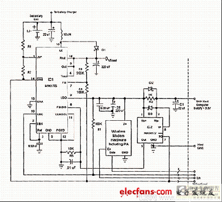
Figure 1. This circuit adds a wireless modem and power amplifier to a handheld device while providing appropriate power management functions.
Tracking the power supply voltage is very important for the interaction between the wireless hardware and the host. This ensures that the bidirectional data and control lines get the correct logic level, and prevents overcurrent from flowing from the main battery to the modem hardware and from the backup battery to the main battery and electronic devices.
This circuit works as follows: First, consider the state of the modem before it is inserted into the PCMCIA slot of the host. There is little or no energy that can be absorbed from the backup battery, so the power to the modem must be disabled in this state. The switch control line of the backup power supply is the PG pin of IC2. Because the VHH voltage of the host that powers IC2 does not exist when the modem is not connected, IC2 is in the off state.
When the power of IC2 is turned off, the power good (PG) output (the internal is an open-drain n-channel MOSFET) is high impedance. At this time, IC2 only absorbs the leakage current. When the PG output is high impedance, two resistor dividers (R6 / R7, monitor the backup battery voltage through IC1 internal comparator, and R3 / R4 set the VBOOST level value when the power is powered on) as the pull-up of the ONB line The resistor turns off the power to IC1. Both IC1's switch-mode boost regulator and low dropout (LDO) regulator are disabled during power off. Therefore, 1μA leakage current flows into IC1 through the voltage divider and 1mA current, and the typical value of the battery leakage current is 2μA.
Consider the power requirements when the power supply is powered up: If the power amplifier (PA) must provide 0.6W and 50% efficiency, 1.2W input power is required. If working at 50% duty cycle (equal transceiver time), then the effective power of the PA is 0.6W. When working at 3.3V, the load draws about 180mA. If the rest of the modem draws 40mA from a 3.3V power supply, the total supply current of the wireless communication link is 220mA1 when the 3.3V power supply is operating.
The IC1 boost regulator can supply (at the VBOOST pin) approximately 800mA at 2.7V power input, and use an intrinsically depleted Li + battery (2.9V to 3.0V) to provide 1A or more. Even so, the internal low-efficiency LDO is used to power the PA and other modem hardware. The LDO current is nominally 300mA and the minimum rating is 220mA. The main reason is the noise suppression problem. When the LDO works at 300kHz, the PSRR value is about 38dB, which is beneficial to suppress the PWM switching noise on the VBOOST pin. The built-in filter of the LDO reduces the requirement for the post-stage noise suppression on the PA supply voltage and the related RF emission part or is not needed at all, so it is easy to pass the Federal Communications Commission (FCC) radiation standard requirements. On the other hand, the intermittent emission efficiency is about 8.3%. VBOOST tracks VHH voltage changes around 3.3V. After the battery is fully charged, the voltage is higher than VBOOST, and when the power is close to depletion, the voltage is lower than VBOOST, so the LDO and boost regulator provide the necessary buck / boost function in order. SEPIC, flyback and forward configurations can also implement buck and boost functions, but they all require bulky and expensive electromagnetic storage elements (transformers) and lack the noise suppression functions provided by LDOs. Based on this consideration, the circuit shown in Figure 1 is superior to other solutions.
The next step is to consider what happens when the modem card is inserted into the host's PCMCIA connector. The function of this step is to make electrical connection between the corresponding circuit ground (GND) and all bidirectional data control lines. The host then uses the EN line to enable or disable the modem hardware. If the EN line is initially low during hardware interaction, then all modem hardware will be disabled and present a high-impedance characteristic to the LDO node.
When the host VHH (normal 3.3V) power source charges C1 through the connector, IC2 receives the power source. The minimum operating voltage of IC2 ensures correct power-up operation, even if VHH is at the lower limit of its range (less than 10% of the normal value). The internal 15μs delay allows VHH to stabilize before the / PG output becomes low (at the V + terminal), and also informs the host that the modem circuit can be enabled via the EN line at this time. / PG low level (virtual ground) makes the dual resistance voltage divider to ground, which can be used to detect the voltage of the battery and boost regulator.
When VHH is connected, IC2 pulls / ONB low when / PG goes low, and IC1 starts to turn off the energy through L1, raising the VBOOST voltage to about 3.7V (via feedback from R3 / R4). Initially, the LDO is turned off and turned on when VBOOST is adjusted. When the LDO output is higher than 2.3V (it should be at 3.3V because VHH has charged C2 through R2) IC1 enters tracking mode. Tracking mode is a special function of IC1, which can force the VBOOST voltage to be 300mV higher than the LDO voltage. This function can be set by connecting the OUT and TRACK pins of IC1. The 300mV margin allows the LDO to remain stable, ensuring the required PSRR even at the maximum output current. Because the voltage is forced to the minimum value required in the tracking mode, the LDO consumes the least battery power.
When the FBLDO pin of IC1 is the internal reference source voltage (typically 1.23V), the LDO is in regulation. The FBLDO voltage is generated by the current through R5, which is proportional to the current through R2. Therefore, IC2 has a transfer function VOUT = gm (VSENSE) R5, where VOUT is the voltage on R5, and VSENSE is the voltage between RS + and RS- (R2), gm = 10-2 mho. When the LDO is adjusted, VOUT = VFBLDO = 1.23V. Therefore VSENSE = VFBLDO / (gm * R5).
Use the relationship VLDO = VHH + VSENSE to replace VSENSE in the above formula,
VLDO = VHH + VFBLDO / (gm * R5).
Substitute the values ​​in the circuit shown in Figure 1,
LDO = VHH + 1.23 / (10-2 * 104) = VHH + 12.3mV.
Set R5 to 10kΩ so that the detection voltage is 12.3mV. According to the above formula, R2 can be selected to program the amount of current from LDO to VHH. For example, R2 = 1kΩ, the current on R2 is about 12μA.
The purpose of using IC2 (high-end current-sense amplifier) ​​is to accurately measure high-end current using low-value high-power, accurate current-sense resistors. This application is not common in the use of 10% accuracy low-power current-sense resistors (such as 1 / 16W surface-mount resistors). We don't care about the exact size of the current from LDO to VHH. We only care about this current as small as possible.
One of the benefits of using a high-value (1kΩ) current-sense resistor is that it only draws about 3.3mA of current from the host through R2 in the case of VLDO short circuit or overload, which is not enough to crash the system. The value of R2 does not have to be 1kΩ; IC2 sinks about 800mA, so setting R2 = 12mV / 800μA = 15W allows the LDO node (not the host) to power IC2.
In another optional configuration, the V + node of IC2 can be directly connected to the LDO instead of VHH. IC2 gets its power from the LDO, except during power-on, when the power supply powers the LDO from VHH to R2. This solution requires the PA and modem hardware to be turned off and presents a high-impedance characteristic to the LDO, so that there is no voltage drop on R2. Similarly, the value of R2 must be small enough to ensure that the V + node has a minimum voltage during normal operation (3V). If VHH = 3.6V or higher, R2 must be less than 375Ωp. This value ensures that IC2 does not exceed a voltage drop of 0.3V at the lower limit of the VHH range (3.6V-10%) at an operating current of 0.8mA.
Schottky diodes (D2, D3) are connected in parallel with R2 to protect IC2 during overvoltage between RS + and RS-. D2 and D3 introduce a small amount of leakage current, which will not affect the operation of the circuit. The capacitor in parallel with R5 bypasses the high-frequency noise of the LDO feedback node to ground, thus ensuring a smooth and stable VLDO voltage. As mentioned earlier, IC1 includes a comparator with variable inputs and outputs. In this circuit, the comparator monitors the backup battery voltage and alerts the host when the remaining power is close to the critical value that can maintain the communication link.
Note that the circuit in Figure 1 is suitable for various conditions in addition to the above. It is compatible with other communication buses and is suitable for interaction between wireless modems and handheld devices. For example, including the board bus and the very popular universal serial bus (USB). The circuit also accepts main supply voltages up to 5V. In order to obtain greater efficiency, in some applications, the PA can be directly connected to VBOOST instead of VLDO. In this way, VBOOST does not need to track VLDO; the two voltages can be controlled separately by separately adjusting the size of the feedback resistor.
IC1 starts at 1.1V and can operate at voltages as low as 0.7V, so it is still acceptable to use two NiMH backup batteries even in boost applications that require lower RF output power levels. Finally IC1 is used as a low-noise PWM regulator with a switching frequency of 300kHz under heavy load. If necessary, the harmonic components of the waveform can be controlled by synchronizing its frequency with an external signal source with a frequency of 200kHz to 400kHz (using the CLK / SEL line). Under light load conditions, the relatively low radiated and conducted energy can force IC1 (also using the CLK / SEL line) into pulse frequency modulation (PFM) mode, which provides the highest efficiency and longest battery life.
Soccer Ball Pump,Football Air Pump,Electric Football Pump,Football Inflator
SHENZHEN SMARTNEWO TECHNOLOGY CO,. LTD , https://www.newopump.com