Domestic LED output value grows rapidly
At present, what are the new changes and new features in the development of LED industry technology at home and abroad?
In terms of global LED output value in 2013, Japan, South Korea, Taiwan, and China each account for about 20%. It should be said that the domestic LED output value is growing rapidly. But relatively speaking, while the domestic output value is growing rapidly, the development level of LED technology is relatively general. On the contrary, the output value of foreign LEDs is generally increasing, and the technological development is very fast.
The main technical indicator of LED is luminous efficiency. According to reports, the LED packaging laboratory of several major companies in the world has exceeded 200lm/w, and the laboratory level of Cree in the United States has reached 303lm/w. We know that the industrialization goal of the US SSL plan is to increase the luminous efficiency of LEDs to 250 lm/w and reduce the price to 0.5 US dollars/klm. The current industrialization level is 120 lm/w~150 lm/w, and the price is about 3 dollars / klm.
In terms of the level of LED lighting, Cree, Philips and other companies have more than 200lm / w, Osram straight tube products have reported to have reached 215lm / w. However, the current level of industrialization in China is only 100lm/w~130lm/w. Of course, the price level is relatively low.
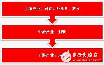
The upstream of the industrial chain continues to break through the increasingly diversified LED packaging
The upstream is the core technology of the LED industry chain. What new developments are there in the core technology?
Peng Wanhua, a well-known expert in the LED industry and deputy head of the semiconductor lighting technology standard working group of the Ministry of Industry and Information Technology, replied: It is true that the upstream of the industrial chain is the core technology of LED. Generally speaking, it includes three parts: substrate, epitaxy and chip. Looking at the substrate first, the key issues currently being developed are lattice matching and thermal matching. Epitaxially grown GaN on the substrate is mainly composed of sapphire (α-Al2O3), SiC, and Si, and has 2, 4, 6 inch wafers and 8 inch Si wafers. Some experts predict that 2015 will be a three-point world of sapphire, Si, GaN homoepitaxial substrates, and in 2016 will be mainly 6-inch wafers.
At the same time, in order to grow higher quality GaN crystals, reduce defects, dislocations, and further reduce costs, the industry is working on new substrates such as 8-inch Si substrates, low-temperature grown GaN homogeneous substrates, and half-poles. And non-polar substrates, dielectric composite substrates, rare earth oxide REO composite substrates, β-Ga2O3 gallium oxide substrates, and the like.
Secondly, epitaxy, epitaxial growth of GaN, InGaAlP and other layers of epitaxy, forming a multi-quantum well structure of PN junction, the main goal is to improve the internal quantum efficiency. At present, the internal quantum efficiency has reached about 60%, and the ultimate goal is to reach more than 90%.
In order to improve internal quantum efficiency and reduce Droop effect, a number of new epitaxial technologies have also been born, such as GaN homoepitaxial, 8-inch Si-based epitaxial, semi-polar non-polar substrate epitaxy, offset epitaxial growth, single Chip polychromatic (R, G, B) epitaxy, epitaxial on composite substrate, etc.
Finally, the chip, the current main goal is to improve the external quantum efficiency, that is, the chip's light extraction efficiency. Do not allow photons to be absorbed multiple times in the crystal, and use various surface treatment techniques on the bottom reflecting surface and the emitting surface.
If distinguished by the light surface and size, LED chips can be divided into a variety of different product forms, the most important are three types, including formal, flip, vertical structure (including film structure). According to the power to distinguish, the low power chip is generally less than 100mw, the medium power chip is generally several hundred mw, and the high power chip is generally above 1w.
Of course, with the development of technology, other structural forms have emerged, such as a 6-sided chip structure, Cree's proprietary DA chip structure (grown GaN on SiC substrate, engraved with V-shaped grooves, currently the world The highest level is the structure), single-chip multi-color light (R, G, B) combined into white light, high-voltage chips and so on.
How do you view the increasing diversification of LED packaging formats?
According to Professor Peng Wanhua, the structure of LED packages has reached more than 100 types, but whether it is Lamp, SMT, COB, PLCC, high-power package (CSP), modular package, etc., the principle of technological development is important. With the development needs of LED application products. The basic content of LED packaging technology is to improve light extraction efficiency, improve light color quality, improve reliability and product cost performance (reduced cost).
If these new packages and technologies are summarized, COB integrated packaging, LED wafer level packaging, COF integrated packaging, LED modular integrated packaging, flip chip packaging technology, and package-free chip technology are all LED light integrated packaging technologies. . Other package structures also have their own characteristics, such as EMC package structure (embedded), EMC package technology (plastic support), COG package (glass substrate), QFN package technology (small pitch pixel unit), 3D package technology, power frame Packaging technology, etc.
Applications focus on three major areas of technology focus on the top ten hot spots
The technological innovation in all aspects of the industrial chain is still for application services. What are the current hot spots in the development of LED application technology?
Peng Wanhua pointed out that at present, the application of LED is still concentrated in three aspects: the first is lighting, including indoor lighting, outdoor lighting, functional lighting, landscape lighting, stage lighting, etc., but nowadays it is still replacing incandescent lamps and energy-saving lamps. The second is the display, including LED display, small-pitch display, backlight (IGZO uses low-power LED), etc. Finally, non-visual lighting, such as ecological agriculture, health care and so on. These have good prospects for development.
Combined with the above applications, the development of LED application technology can be summarized into ten hot issues.
First, the total energy efficiency of LED light sources and lamps. Total energy efficiency = internal quantum efficiency & TImes; chip light extraction efficiency & TImes; package light efficiency & TImes; phosphor excitation efficiency & TImes; power efficiency × lamp efficiency. At present, this value is less than 30%, and our goal is to make it greater than 50%.
Second, it is the comfort of the light source. Specifically, it includes color temperature, brightness, color rendering, color tolerance (color temperature uniformity and color drift), glare, and no flicker, but there is no uniform standard.
Third, the reliability of LED light sources and lamps. Mainly life and stability issues, to ensure product reliability from all aspects, to achieve a service life of 20,000 to 30,000 hours.
Fourth, it is the modularization of LED light sources. The modularization of the LED light source system integrated package is the development direction of the semiconductor illumination source. The key component of the problem is the optical component interface and the driving power supply.
Fifth, it is the safety of LED light source. To solve problems such as light bio-safety, super bright, and light flicker, especially stroboscopic problems.
Sixth, it is modern LED lighting. LED lighting source and lighting should be simple, beautiful and practical. It adopts digital and intelligent technology to make the LED lighting environment more comfortable and more suitable for individual needs.
Seven, is intelligent lighting. Combined with communication, sensing, cloud computing, and Internet of Things, LED lighting can be effectively controlled to achieve multi-functional lighting and energy saving, and improve the comfort of the lighting environment. This is also the main development direction of LED applications.
Eight, is a non-visual lighting application. In this new field of LED applications, it is predicted that its market size is expected to exceed 100 billion yuan. Among them, ecological agriculture includes plant breeding, growth, livestock and poultry breeding, pest control, etc.; health care includes treatment of certain diseases, improvement of sleep environment, health care function, sterilization function, disinfection, purification of water and so on.
Nine is a small pitch display. At present, its pixel unit is about 1mm, and it is developing P0.8mm~0.6mm products, which can be widely used in high-definition and 3D display, such as projector, command, dispatch, monitoring, large-screen TV, etc.
Ten is to reduce costs and improve cost performance. As mentioned above, the target price of LED products is 0.5 USD/klm. Therefore, new technologies, new processes, and new materials should be adopted in all aspects of the LED industry chain, including substrate, epitaxy, chip, package, and application design. , so that the cost continues to decline, improve cost performance. In this way, we can finally provide people with energy-saving, environmentally friendly, healthy and comfortable LED lighting environment.
Robotic Vacuum Cleaner,Quiet Robotic Vacuum Cleaner,Top Robotic Vacuum Cleaners, Intelligent Robotic Vacuum Cleaner
NingBo CaiNiao Intelligent Technology Co., LTD , https://www.intelligentnewbot.com