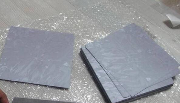
**What is a Solar Wafer?**
A solar wafer is a thin slice of silicon that serves as the foundation for photovoltaic (PV) cells, which convert sunlight into electricity. These wafers are typically made from crystalline silicon, either monocrystalline or polycrystalline, and are used to produce standard solar panels. However, there are also other types of solar cells, such as thin-film, amorphous silicon, and concentrated photovoltaic systems, which use different materials and manufacturing methods.
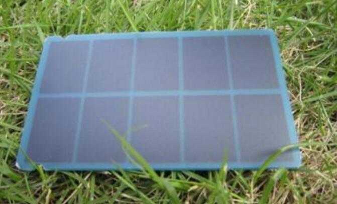
Once the solar wafer is integrated into a panel, it captures sunlight and converts it into usable electrical energy. This process is highly efficient and environmentally friendly, making solar power a reliable and sustainable energy source. With advancements in technology, solar wafers have become more cost-effective and widely adopted across various industries.
**How Do Solar Wafers Work?**
When sunlight hits a solar wafer, photons from the light strike the semiconductor material, usually silicon, creating electron-hole pairs. These charge carriers move through the PN junction formed within the wafer, generating an electric current. This process is known as the photovoltaic effect.
One method of producing solar wafers involves using a ribbon polycrystalline silicon process. In this approach, a thin silicon ribbon is pulled directly from molten silicon and then cut into square shapes using laser technology. This technique reduces material waste and improves efficiency compared to traditional mechanical cutting methods.
**The Production Process of Solar Wafers**
1. **Rounding and Squaring**
The silicon single crystal rod is cut into a quasi-square shape, and the corners are rounded using a roller mill to prepare it for further processing.
2. **Pickling**
The quasi-single-crystal rod is immersed in an acid solution to remove surface impurities and contaminants, ensuring a clean base for the next steps.
3. **Adhesive Bonding**
The cleaned silicon rod is bonded onto a workpiece plate to facilitate handling during the slicing process.
4. **Slicing**
The bonded rod is placed on a cutting station and sliced into individual wafers based on specific process parameters.
5. **Cleaning and Degumming**
After slicing, the wafers are pre-cleaned to remove any residual cutting fluid and then degummed to eliminate any remaining adhesives.
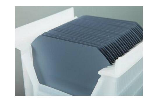
6. **Ultrasonic Cleaning**
The wafers are placed in a cassette and cleaned in an ultrasonic bath to remove microscopic particles and impurities.
7. **Drying**
The cleaned wafers are dried using centrifugal force and heat to ensure they are completely dry before inspection.
8. **Inspection and Packaging**
Each wafer undergoes thorough testing for appearance, thickness, resistivity, TTV (Total Thickness Variation), and warpage. Based on these tests, the wafers are graded and packaged according to quality standards and delivery requirements.
**Are Solar Wafers Radioactive or Toxic?**
While silicon itself is not toxic, the production of solar wafers involves certain chemicals and processes that can be hazardous if not properly managed. For example, some cleaning agents and etching solutions used during manufacturing may contain harmful substances. Additionally, during the fabrication of high-density integrated circuits, silicon wafers may come into contact with materials like lead, which can be toxic when soldered.
However, once the solar wafers are fully processed and assembled into panels, they are generally safe and non-toxic. The radiation risk during production is minimized through proper safety protocols and environmental controls. Overall, solar wafers are considered a clean and sustainable energy solution, with minimal long-term environmental impact.
Dot Matrix Led Display,Round Dot Matrix Led Display,5X7 Dot Matrix Led Display,1.2 Inch 5X7 Dot Matrix Display
Wuxi Ark Technology Electronic Co.,Ltd. , https://www.arkledcn.com